PCB auto routing
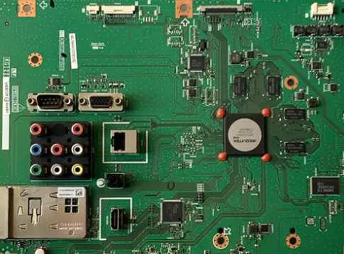
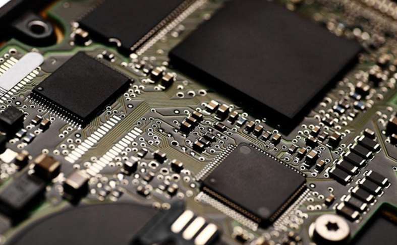
In order to obtain the best performance of electronic circuits, the layout of components and wires are very important, and wiring as the top priority of PCB design process, which will directly affect the performance of PCB board.


In order to obtain the best performance of electronic circuits, the layout of components and wires are very important, and wiring as the top priority of PCB design process, which will directly affect the performance of PCB board.
The role of PCB board is not only to combine scattered components, but also to ensure the regularity of circuit design, a good way to avoid the chaos and error caused by manual wiring and wiring.
Almost all PCB design software includes a tool called an autocabler, but the autocabler never does the wiring for itself.
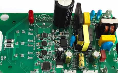
Considering the performance and processing efficiency of PCB, the preferred process sequence is as follows: 1. If the component surface is mounted on one side, it is formed by reflow welding; 2. 2. If the component surface patch and plug-in are mixed: one
The PCB process design requirements are introduced in detail: 1, test point addition, 2, optical location point, 3, add working edge, 4, film file output, 5, plate rules, 6, board information annotation
PCB design impedance matching: PCB design impedance matching refers to a suitable collocation between the signal source or transmission line and the load. According to the access mode PCB design impedance matching has serial and parallel two ways; Accordi
Polygon filling deviation usually occurs when polygon plating copper on multi-grid circuit boards. While it does not have a standard based on a single grid, it can provide service beyond the required life of the boards.
Circuit board design required data: 1. Circuit diagram, necessary, 2. Circuit consumption power calculation, not necessary, 3. Circuit diagram Electrical list, not required, 4. Component table, required, 5. Circuit board design drawing, required, 6. Circu
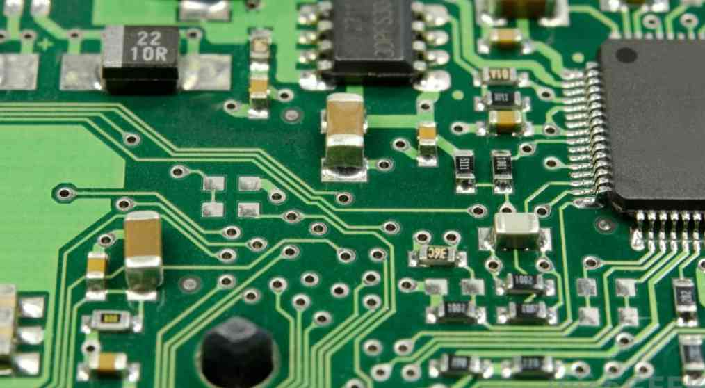
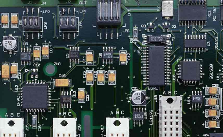
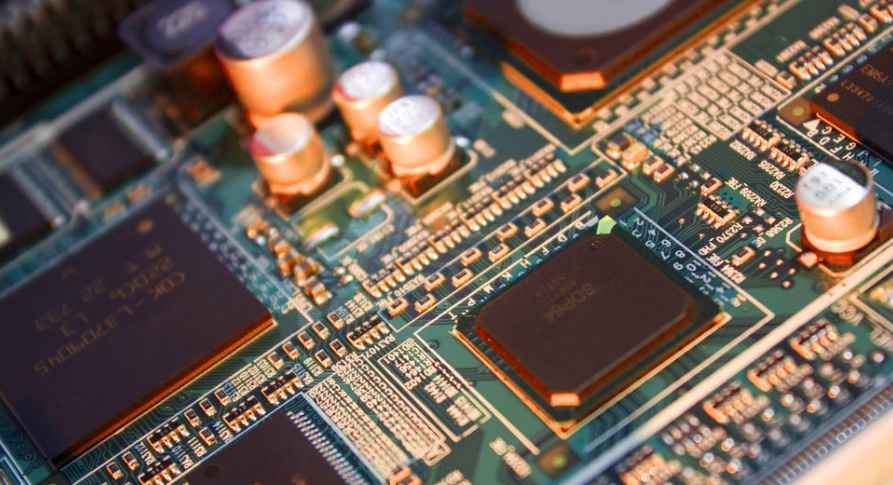
Width and spacing of printed wire are important design parameters, which affect not only the electrical performance and electromagnetic compatibility of PCB board, but also the manufacturability and reliability of PCB board.
The performance index of high frequency circuit directly affects the quality of the whole product. The layout and wiring of components can maximize the performance index of the circuit and achieve the design purpose of anti-interference.
Circuit board design and production process: 1. Preparation of production materials, 2. Circuit board production and manufacturing, 3. Production and design
Preliminary work to be done before PCB design :1, determine the number of PCB layers, 2, PCB design rules and restrictions, 3, component layout


