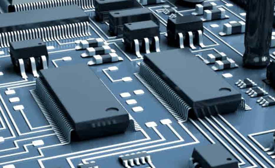
Why should capacitors be placed nearby in PCB design?
The method of high-speed PCB design and wiring to solve signal crosstalk: First, in possible cases to reduce the signal along the conversion rate usually in the device, while meeting the design specifications as far as possible to choose slow devices, and