
Контрактное производство электроники под ключ в Китае
Шэньчжэнь, район Баоань, улица Фуюн, улица Фуцяо, район 3, промышленный парк Лонгхуй 6

Printed circuit boards are an integral part of many electronic devices. If you plan to purchase PCBS, you should learn more about the design process. In this way, you can ensure that the board is perfectly suited for your desired application. In addition, you will optimize the cost and maximize the price of the board. The following to introduce the basic PCB elements and PCB design and production process.
I. Overview of basic PCB elements
Before we discuss what you need to know about PCB design and manufacturing, we'll walk you through the basic components of each printed circuit board.
1.1. Layers
Each board contains layers, and the number of layers you choose depends on the application you need. As a general rule, the more layers you choose, the more complex the PCB becomes.
That's why building more layers of boards can take more time, though established companies still make them quickly.
Here are some common choices people make when assembling PCBS:
Two-layer - a board that is relatively easy to make and used for simple products such as toys;
Four Layers - solutions that many people use for Internet of Things (IoT) projects;
Six to eight layers -- you'll see these in tech-related devices like smartwatches and smartphones.
If you are sure you are looking for the simplest solution, the manufacturer will also accept single-layer boards.
You can also use more than eight layers, but make sure your application needs that many. Otherwise, you'll end up paying more for no reason.
1.2. Dimensions and thickness
Next, you need to determine the size and thickness of the board. As for size, the only important factor to consider is that it fits perfectly into your application.
This is why you should consider the size of the product and measure the space you plan to place the PCB in.
You must measure the dimensions accurately because there is not much margin for error if you want your product to work properly.
In terms of thickness, it can vary from about 0.5 mm to 2.5 mm. You should consider your application and decide accordingly, but the average thickness is about 1.2-1.8mm.
1.3. Other things to consider
Here is a list of other components and features you might want to consider when ordering your PCB:
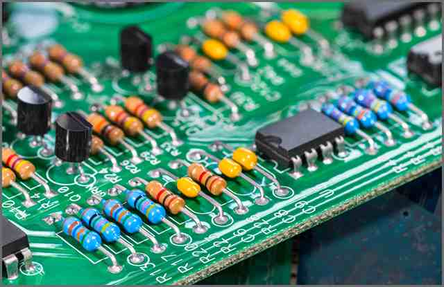
Materials - Common choices include standard FR4, FR4-TG170, and halogen-free materials.
Color - You can use red, green, yellow, blue and other colors of solder resistance layer.
Finish - Lead-free or leaded HASL, different dips of silver, gold and tin are available.
Copper Weight - You can choose the desired thickness of each layer, ranging from 0.5 oz to 4 oz. Copper is used because of its high electrical conductivity.

Ii. pcb Design and manufacture --Design Process
The design process begins with the design of the circuit. The first thing you need to do is take out a document called a schematic. You can think of it as a blueprint that shows in detail all the components and how they communicate.
You can design circuits on a PC using professional software (such as Quadcopter, Altium, ExpressPCB, or many others available online).
Keep in mind that most of these tools are paid versions, so you'll have to purchase them if you want to design your own PCBS.
What you need to know about PCB design and manufacture is the specification of each component to be included on the board. Schematics can greatly help with the next step, which is the PCB layout.
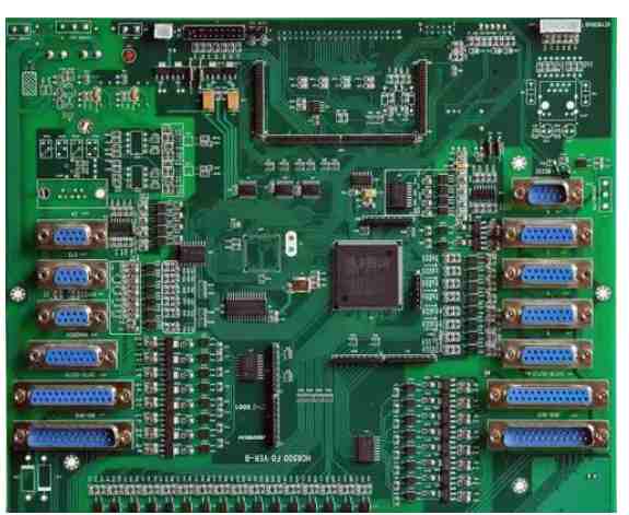
PCB design and manufacture
2.1. Assign components to their locations
Each component needs to have a precise position in the manufacturing process. This is why creating a board layout is a crucial step in PCB design.
This can be tricky because you need to find the best fit for all the components and explain how to wire them. This is why assembling PCBS with more layers is more challenging.
Most designers adopt a strategy of using different areas for different purposes.
The components associated with the power supply are in one section, the audio output is in another, and so on. Grouping is crucial because it saves space and controls noise and interference.
Leds, connectors, audio jacks, and other important user experience items must be considered. You want to maximize availability so that you can use the PCB effortlessly.
The final step is to generate a Gerber file, which is a standard printed circuit board manufacturing format.
You might think that designing a PCB is easy, but it's tricky to place all the components correctly.
You need to avoid interference and other potential problems while maximizing the user experience, and only a professional PCB design firm can do this job.
3. pcb design and manufacture --Manufacturing Process
Once the PCB design is ready, it is ready to be manufactured. The easiest way to do this is to send the Gerber file to the manufacturer and let them work their magic.
They will use layouts to assemble PCBS and turn ideas into reality. If you choose a professional manufacturer, they will most likely have all the necessary materials ready.
This would eliminate the need to order materials and wait for delivery. Instead, they can start making them right away.
3.1. Install PCB components
The main task in the assembly process is to attach the component to the board surface. There are two ways to do this:
Surface Mount Technology (SMT) is very convenient in manufacturing many PCBS. Reliable and fast professional tools handle installation to ensure that there is no room for human error while speeding up the process.
Through Hole - Some prefer to manually mount components to the board surface, but this usually takes more time than SMT.
Interestingly, SMT does not support all components. If the item you choose is not a standard size or otherwise, you may have to install the feature manually. This is why companies often use a combination of the above methods.
3.2. pcb design and manufacturing --Soldering
When welding is required, the manufacturer will use one of the following methods:
Reflow soldering - This technique is ideal for permanently attaching components to the circuit board.
Wave - This welding is convenient when manually installing details.
Iron - A large number of manufacturers rarely use this form of welding.
In the end, the manufacturer may only make a sample circuit board to test its quality. After thorough testing and necessary modifications, mass production will begin.
kingford is a professional PCB design company engaged in electronic products layout layout design, mainly undertake multi-layer, high density PCB design and circuit board design proofing business. Proficient in the use of market mainstream PCB design software, professional and efficient communication to ensure PCB design progress
Nine basic principles of SMB design
2023-02-23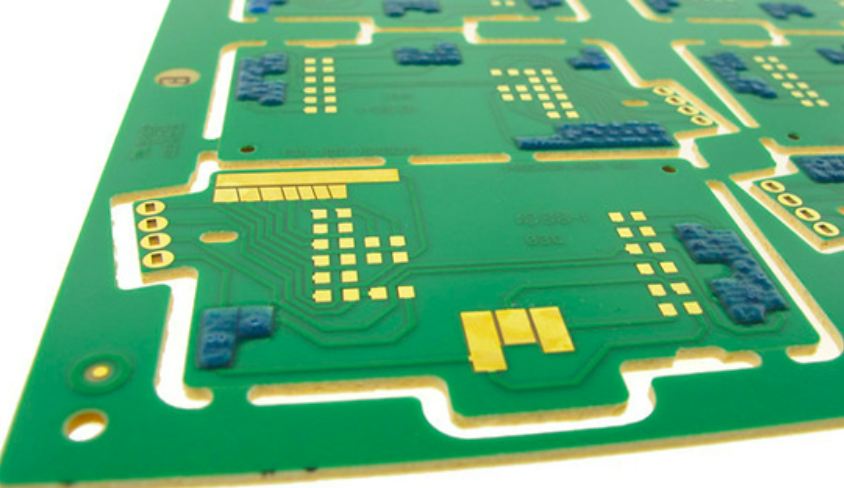


Достаточно загрузить файлы Gerber, BOM и проектные документы, и команда KINGFORD предоставит полное предложение в течение 24 часов.