
Контрактное производство электроники под ключ в Китае
Шэньчжэнь, район Баоань, улица Фуюн, улица Фуцяо, район 3, промышленный парк Лонгхуй 6

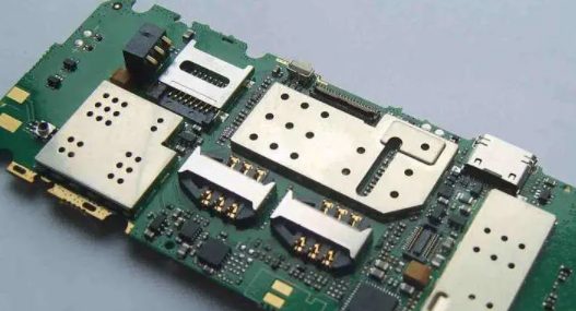
In multi-layer PCB design, GND layer and power layer are indented to a certain extent. Why should they be indented? Next, Shenzhen PCB Design Company will introduce the reasons for the indentation design of GND layer and power layer in the following multi-layer PCB design.
To figure this out, we need to first understand the "20H" rule:
The 20H principle is mainly proposed to reduce the electromagnetic radiation problem of the circuit board. If there is a high speed current on the circuit board, there is a magnetic field associated with it, at the edge of each layer.
When the upper and lower planes of the stratum and the power layer are the same size, electromagnetic interference will be radiated outward at the edge of the plate due to the change of electric field between the stratum and the stratum. Generally, the solution is to shrink a certain distance inside the power layer, so that the electric field can only be conducted within the range of the stratum, so as to inhibit the edge radiation effect. Improve electromagnetic compatibility (EMC).
Then, how much distance should we generally shrink? The distance we shrink is the distance of "20H" we said before, and this H refers to the thickness of the medium between the power layer and the ground. The adoption of "20H rule" is to ensure that the edge of the power plane should be shrunk at least 20 times as much as the interval between the two planes than the edge of the 0V plane.
After the indented power plane and ground plane, we can see that most of the electromagnetic field will not radiate out, thus reducing the external EMI radiation. But why do we say that most of the electromagnetic field will not radiate out? Because we found that when the power source is indent by 20 hours relative to the edge of the formation, the density of the electromagnetic field can be reduced by about 70 percent, not that it can be reduced to zero, but if we need to contain more electric field, we can indent by 100 hours. Generally speaking, indent by 100 hours can contain 98 percent of the electric field. So that's one reason why our boards need to be indented.

However, due to the laminated design, PCB wiring cannot be carried out if 20H is strictly met on some common PCB boards. Therefore, the general treatment method is that the GND of the power supply is reduced by 1MM relative to GND, so that the performance of our boards can be guaranteed to a certain extent.
We also need to note that our 20H principle can have obvious effects only under certain conditions.
1. The power plane shall be located inside the PCB, and the upper and lower layers adjacent to it shall be 0V planes, and the distance between the two 0V planes shall be at least 20 times of the distance between them and the power plane.
2. The total number of PCB layers shall be greater than or equal to 8 layers.
2. What is the difference between aluminum substrate and FR4 plate?
Published :2022-12-20 17:05 Read :77 Source: Technical article editor: Shenzhen kingford PCB board Department
Aluminum substrate and FR4 board is a common circuit board, so what is the difference between aluminum substrate and FR4 board? The next Shenzhen PCB board factory -kingford for you to introduce.
2. What is the difference between aluminum substrate and FR4 plate?
The difference between aluminum substrate and FR4 plate
1. Different performance
The comparison of wire (copper wire) and fuse current on different substrate materials, from the comparison of aluminum substrate and FR-4 plate, due to the high heat dissipation of metal substrate, the conduction is significantly improved, from another Angle to illustrate the high heat dissipation characteristics of aluminum substrate. The heat dissipation of aluminum substrate is related to its insulating layer thickness and thermal conductivity. The thinner the insulation layer, the higher the thermal conductivity of the aluminum substrate (but the lower the voltage resistance).
2. Different machinability
Aluminum substrate has higher mechanical strength and toughness than FR-4 plate. For this purpose, large area printed boards can be made on aluminum substrates on which large components can be mounted.
3. Electromagnetic shielding performance is different
In order to ensure the performance of the circuit, some components in electronic products need to prevent the radiation and interference of electromagnetic waves. Aluminum substrate can be used as shielding plate to shield electromagnetic wave.
4. Different coefficient of thermal expansion
Due to the thermal expansion of FR-4 in general, and of plate thickness in particular, the quality of the metallized holes and wires is affected. The main reason is that the thermal expansion coefficient thickness of copper in raw materials is 17 * 106cm/cm-C, FR-4 plate is 110 * 106cm/cm-C, the difference is large, easy to produce heating substrate expansion and change of copper wire and metal hole rupture damage to product reliability. The thermal expansion coefficient of aluminum substrate is 50×106cm/cm-C, smaller than common FR-4 plate, close to the thermal expansion coefficient of copper foil. This helps to ensure the quality and reliability of the printed circuit board.
5. Different application areas
FR-4 board is suitable for general circuit design and common electronic products. Aluminum substrate is often used for electronic products with high heat dissipation requirements, such as LED lamp board.
Shenzhen kingfordPCB design capability
Maximum signal design rate: 10Gbps CML differential signal;
Maximum number of PCB design layers: 40;
Minimum line width: 2.4mil;
Minimum line spacing: 2.4mil;
Minimum BGA PIN spacing: 0.4mm;
Minimum mechanical hole diameter: 6mil;
Minimum laser drilling diameter: 4mil;
Maximum number of pins:; 63000 +
Maximum number of components: 3600;
Maximum number of BGA: 48+.
kingford Electronics is a professional PCB design company engaged in electronic products layout layout design, mainly undertake multi-layer, high density PCB design and circuit board design proofing business. With an average of more than 10 years of work experience in PCB design team, skilled use of market mainstream PCB design software, professional and efficient communication to ensure the progress of PCB design, help you to seize the market opportunity earlier!


Достаточно загрузить файлы Gerber, BOM и проектные документы, и команда KINGFORD предоставит полное предложение в течение 24 часов.