
Контрактное производство электроники под ключ в Китае
Шэньчжэнь, район Баоань, улица Фуюн, улица Фуцяо, район 3, промышленный парк Лонгхуй 6

1. Background description
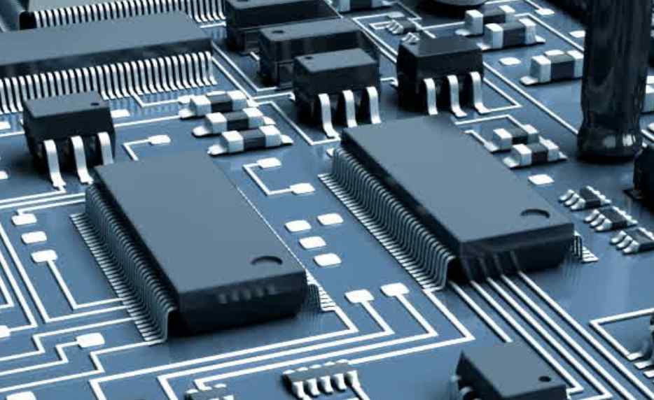
PCBA welding adopts hot air reflow welding, which relies on the convection of wind and the conduction of PCB, pad and lead for heating. Due to the different heat capacity and heating conditions of the pad and pin, the temperature of the pad and pin at the same time in the reflow welding heating process is also different. If the temperature difference is relatively large, it may cause poor welding, such as QFP pin welding, rope suction; Tablet component stele and displacement; BGA solder joint shrinkage fracture, etc. Similarly, we can solve some problems by changing the heat capacity.
2. Design requirements
(1) Thermal design of heat sink pad.
In the welding of heat sink element, the phenomenon of less tin in heat sink pad will be encountered, which is a typical application situation that can be improved by heat sink design. For the above situation, it can be designed by increasing the heat capacity of the heat dissipation hole. The heat dissipation hole is connected to the inner grounding layer. If the grounding layer is less than 6 layers, a partial heat dissipation layer can be isolated from the signal layer while the aperture is reduced to the minimum available aperture size.
(2) Thermal design of high-power grounding jack.
In some special product designs, cartridge holes sometimes need to be connected to multiple ground/level surfaces. Because the contact time between the pin and the tin wave during wave soldering is very short, that is, the welding time is often 2~3s. If the heat capacity of the jack is relatively large, the temperature of the lead may not meet the requirements of welding, forming cold welding points. To avoid this, a design called the starmoon hole is often used, where the weld hole is separated from the earth/electric layer and a large current is passed through the power hole.
(3) Thermal design of BGA solder joint.
Under the conditions of mixing process, there will be a unique phenomenon of "shrinkage fracture" caused by unidirectional solidification of solder joints. The fundamental reason for the formation of this defect is the characteristics of the mixing process itself, but it can be improved by optimizing the design of BGA corner wiring to make it slow cooling.
According to PCB processing experience, generally the solder joints with shrinkage fracture are located at the corner of BGA. It can be synchronized with other solder joints or cooled later by increasing the heat capacity of BGA corner solder joints or reducing the heat conduction velocity, so as to avoid the phenomenon of being broken under the buckling stress of BGA caused by cooling first.
(4) Design of plate element pad.
With the smaller and smaller size of chip components, more and more phenomena such as displacement, stele and turnover. These phenomena are related to many factors, but the thermal design of the pad is one of the most influential aspects. If one end of the pad is connected with a wide wire, and the other end is connected with a narrow wire, then the heating conditions on both sides are different. Generally speaking, the pad connected with a wide wire will melt first (this is contrary to the general expectation that the pad connected with a wide wire will melt because of its large heat capacity, in fact, the wide wire becomes a heat source, Depending on how the printed circuit board is heated), surface tension at the melted end can also shift or even flip components.
Therefore, it is generally expected that the width of the wire connected with the pad should not be greater than half the length of the connected pad edge as far as possible.
(5) Influence of wave crest welding on component surface.
BGA.
Most pins of BGA with pin center distance of 0.8mm and above are connected to the line layer through the pilot hole. In wave soldering, heat is transferred through the pass hole to the BGA solder spot on the element surface. Depending on the heat capacity, some do not melt, some semi-melt, easy to fracture failure under the action of thermal stress.
Chip capacitor.
Chip capacitors are very sensitive to stress and are prone to cracking due to mechanical and thermal stresses. With the widespread use of wave soldering for pallet selection in PCB design, the chip element at the window boundary of the pallet is easy to break due to thermal stress.
PCB board design of the 8 basic principles
2023-02-25


Достаточно загрузить файлы Gerber, BOM и проектные документы, и команда KINGFORD предоставит полное предложение в течение 24 часов.