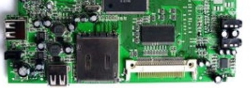
PCB high speed signal circuit design specification skills
A perfect PCB board not only needs to do the component selection and setting is reasonable, but also needs to have good signal conduction performance.


A perfect PCB board not only needs to do the component selection and setting is reasonable, but also needs to have good signal conduction performance.
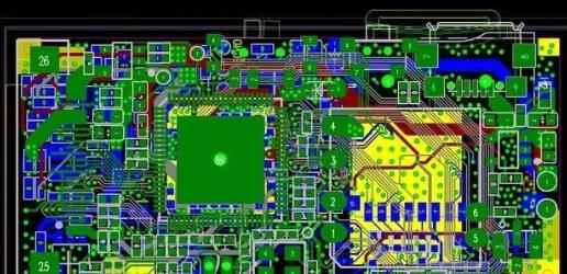
The basic PCB design process is as follows: preliminary preparation →PCB structure design → mesh guide → rule setting →PCB layout → Wiring → routing optimization and silk screen → network and DRC inspection and structure inspection → output light drawing
The design of PCB starts from determining the size of the board. The size of PCB is limited by the size of the case shell, so that it can be placed into the shell exactly. Secondly, the connection mode of PCB and external components should be considered.
Solutions to impedance discontinuity problems in PCB design: 1. Gradient line, 2. Corner, 3. Large pad, 4. Through hole, 5. Through hole coaxial connector
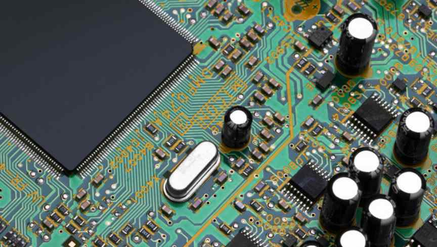
As an electronic engineer design circuit is a necessary hard work, if the PCB design is not reasonable performance will be greatly compromised.
Four difficulties in the production and processing of multilayer circuit board: 1, the inner line production difficulties, 2, the inner layer between the point of difficulty, 3, pressing process difficulties, 4, drilling production difficulties
SMT patch BOM list arrangement Note: 3. The description must be clear. 4. There are some crucial electronic components. Considering the fluctuations of the component market and the cost, 5. 6. Coordinate values required by coordinate T/B to distinguish po
There are three PCB design methods that can withstand 100A current:1: PCB wiring, 2: terminals, 3: custom copper bar, 4: special process
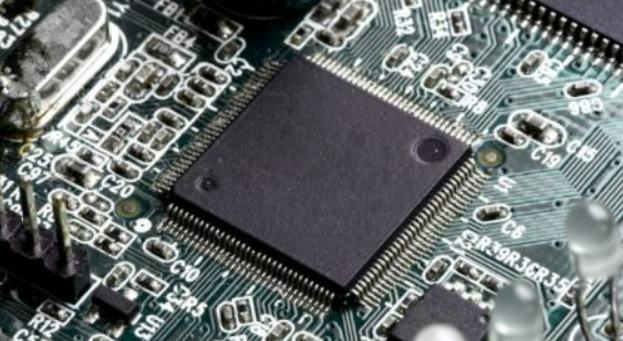
It is strongly required in various PCB design guidelines that high frequency and high speed signal transmission lines need to maintain consistent characteristic impedance, and that 90° Angle routing at the corner of the transmission line will change the l

The circuit board software designed by many circuit board designers is designed according to the components of the circuit board software itself.

The calibration shall be carried out by an approved standard measuring institution. The quality assurance department shall register the calibrated equipment, instruments and tools and keep a calibration record book.
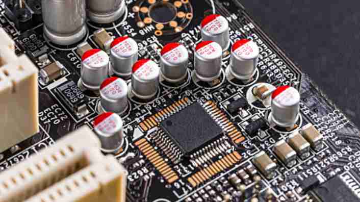
Whether in the manufacturing and assembly process or in actual use, PCB to have reliable performance, this is very important.


