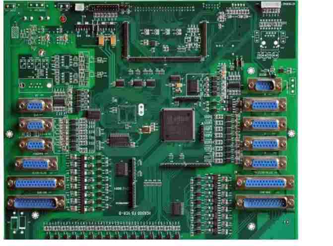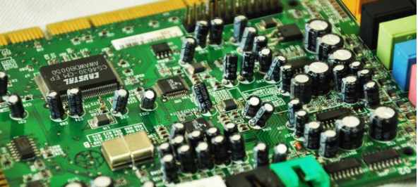
Before introducing PCB window design, we first need to know what the solder resistance layer is. Solder resistance layer refers to the part of the PCB board to be inked, used to cover the wiring and copper, to protect the metal elements on the PCB and prevent short circuit. Welding resistance window refers to opening an opening on the welding resistance layer so as to weld at the opening position. Simply speaking, window opening is the position without ink cover. All the positions without printing solder can be called window, do not print solder position has welding PAD, patch pad, groove position and so on. There is also a case called half window, half window is the welding disc part is not covered with welding resistance film, part is covered with welding resistance film.
How to distinguish "through hole opening window" and "through hole cover oil"?
In PCB design, you may often hear the terms "through the hole window" and "through the hole cover oil". In fact, it is literally, a hole to open the window, a hole to cover the oil. In other words, whether to insulate the PCB surface.
Window-opening means that it is easy to tin the position of window-opening, and it can be judged whether to open the window according to whether it can tin. Cover oil, refers to when the patch is not easy to tin, this is determined by the process. The reasons why there is no oil covered through the hole are as follows: because the welding resistance oil is liquid and the middle of the hole is empty, it is easy for the welding resistance oil on the welding ring to enter the hole during the roasting process, which leads to the occurrence of yellow through the hole. This situation is related to the concentration of welding oil, the oven and the application force, so some of them can appear green. And then there are the ones that don't.
Why weld the window?
For the hole, if the window is not opened, the solder resistance layer ink will enter the hole. For some holes that do not need ink plug holes, it is necessary to design it as a window through the hole. For components with through-hole installation, if the PCB is not soldered to the window, the components cannot be properly welded to the board. Aperture window is not only convenient for welding, but also can be measured on the hole. For some special positions of the hole welding window, you can use a multimeter to measure on the hole.
For PCB, if the window is not opened, surface treatment can not be carried out, tin spraying, welding can not be carried out.
How to weld the window?
1. The welding pad will open a window by default in the PCB design (OVERRIDE: 0.1016mm), that is, the welding pad is exposed to copper foil, the outer extension is 0.1016mm, and the wave soldering tin plating. No design changes are recommended to ensure weldability.
2. The overhole will be windowed by default in PCB design (OVERRIDE: 0.1016mm), that is, overhole copper foil, external expansion of 0.1016mm, tin during wave soldering. If designed to prevent over-hole tinning and not expose copper, you must check the PENTING option in the additional properties of the SOLDER MASK to close the over-hole.
3, in addition, this layer can also be used separately for non-electrical wiring, then welding green oil corresponding window. If it is on the copper foil wire, it is used to enhance the current of the wire. When welding, it can be tinned. If it is on non-copper wire, it is usually designed to do signage and special character silk screen printing, which can save production.

2. Do you know the production difficulties of multi-layer PCB proofing?
multilayer PCB board in communication, medical, industrial control, security, automobile, electric power, aviation, military, computer and other fields as the "core force", the product function is more and more, the line is more and more intensive, so relatively, the production is more and more difficult.
At present, the domestic PCB manufacturers that can mass-produce multi-layer circuit boards often come from foreign enterprises, only a few domestic enterprises have the strength of batch. The production of multilayer circuit board not only requires higher technology and equipment investment, but also needs experienced production and technical personnel. At the same time, it is strict and tedious to obtain the customer certification of multilayer circuit board. Therefore, the entry threshold of multilayer circuit board is higher and the industrialization production cycle is longer. Specifically, the processing difficulties encountered in the production of multilayer circuit boards are mainly the following four aspects.
Multilayer circuit board in the production and processing of four difficulties
1. Difficulty in making the inner circuit
Multilayer circuit has special requirements of high speed, thick copper, high frequency, high Tg value, and more and more requirements for inner wiring and graphic size control. For example, ARM development board has a lot of impedance signal lines in the inner layer, so it is more difficult to ensure the integrity of the impedance.
There are many signal lines in the inner layer, and the width and spacing of the lines are basically about 4mil or less. The thin production of laminated multi-core plate is easy to wrinkle, and these factors will increase the production cost of the inner layer.
2. Difficulty of alignment between inner layers
With the increasing number of multilayer layers, the alignment requirements of the inner layer are also higher and higher. Film will grow and shrink under the influence of ambient temperature and humidity in the workshop, and the core board will grow and shrink in the same way when produced, which makes the alignment accuracy between the inner layers more difficult to control.
3. Difficulties in the pressing process
The superposition of multiple core plates and PP (semi-cured sheet) is prone to problems such as delamination, slide plate and drum residue when pressed. Because of the large number of layers, the volume control and size coefficient compensation cannot be consistent. If the insulation layer between layers is thin, it is easy to cause the failure of inter-layer reliability test.
4. Difficulties in drilling production
The multi-layer board uses high Tg or other special plates, and the roughness of the drilling of different materials is not the same, which increases the difficulty of removing the rubber slag in the hole. High density multilayer plate has high hole density, low production efficiency and easy to break the knife. Too close hole edge between holes of different networks will lead to CAF effect.
Therefore, in order to ensure the high reliability of the final product, it is necessary for the multilayer manufacturer to carry out corresponding control in the production process.
Shenzhen kingford is a PCB design company specializing in layout design of electronic products, mainly engaged in multi-layer and high-density PCB design and circuit board design proofing business, skilled in using the market mainstream PCB design software, professional and efficient communication to ensure the progress of PCB design. Help you seize the market opportunity one step earlier!


