
Контрактное производство электроники под ключ в Китае
Шэньчжэнь, район Баоань, улица Фуюн, улица Фуцяо, район 3, промышленный парк Лонгхуй 6

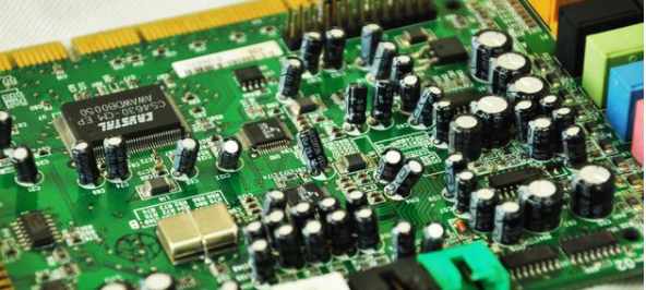
Mark points, also called reference points, provide a common locatable circuit pattern for all steps in the SMT assembly process. Mark point is very important for SMT processing and production. Next, Shenzhen kingford SMT patch manufacturer will introduce the design specification of Mark point in PCB design.
1. Function and category of MARK point
MARK point classification:
1. Single board MARK, whose function is to locate the position of all circuit characteristics on a single board, is essential;
2. The plate MARK is used to assist positioning of all circuit features on the plate and assist positioning;
3, local MARK, its role is to locate the reference point MARK of a single component, in order to improve the mounting accuracy (QFP, CSP, BGA and other important components must have local MARK), essential;
2. MARK Point design specification
All incoming SMT boards must have Mark points, and the relevant specs of Mark points are as follows:
1. Shape: Mark point is required to be a solid circle.
2. Composition: A complete MARK point includes: mark points (or feature points) and empty areas.
3. Location
Mark points are located diagonally relative to each other on a circuit board or assembly board and are separated as far apart as possible. Preferably distributed in the longest diagonal position;
In order to ensure the mounting accuracy, SMT requirements are as follows: for all types of machines (including derivative types) on the SMT test run since Jan-01-06, there must be at least one pair of MARK points in each 1pcsPCB that meet the design requirements and can be recognized by SMT machines, that is, there must be a single MARK. The spliced MARK or combined MARK only serves as an aid to positioning
When assembling boards, the relative positions of MARK points on each board must be the same. Do not move the position of the MARK point on any board for any reason, resulting in the asymmetry of the position of the MARK point on each board;
All marks on the PCB board are valid only if they are two marks on the same diagonal and appear in pairs. Therefore, MARK points must be paired before they can be used.
4. Size
The minimum diameter of the Mark point marker is 1.0mm[0.040"] and the maximum diameter is 3.0mm [0.120"]. The size of the Mark dot shall not vary more than 25 microns [0.001"] on the same printed board;
Special emphasis: the size of all Mark points on the PCB of the same board number must be the same (including PCB of the same board number produced by different manufacturers);
You are advised to set the diameter of Mark points in all RD-layout files to 1.0mm.
5. Edge distance
The Mark point (edge) must be ≥5.0mm[0.200"] from the edge of the printed board (minimum machine-clamped PCB spacing requirement), and must be inside the PCB board rather than on the board edge, and meet the minimum Mark point clearance requirement. Emphasis: The distance between the edge of MARK point and the edge of the plate is ≥5.0mm[0.200"], but not the center of MARK point.
6. Requirements for emptiness
Around the Mark mark, there must be an open area with no other circuit features or markings. The circle radius of open area r≥2R, r is the radius of MARK point, when r reaches 3R, the machine recognition effect is better. It is often found that the open area of MARK point is blocked by the character layer or cut by V-CUT, resulting in the SMT machine cannot recognize.

7. Materials
The Mark point mark may be bare copper, clear anti-oxidation coating protected bare copper, nickel or tin plating, or solder coating. If soldermask is used, the Mark point or its open area should not be covered.
8. Flatness
The surface flatness of the Mark point should be within 15 microns [0.0006"].
9. Contrast
The best performance is achieved when there is high contrast between the Mark mark and the substrate material of the printed board.
The inner background must be the same for all Mark points.
2. Arrange the SMT patch BOM list for precautions
BOM is the abbreviation of Bill of Material. In Chinese, BOM means bill of Materials. As the name suggests, it is a list of all the materials used in the processing of a product. Therefore, BOM list is very important for SMT patch factory, which contains important information in the whole product processing process.
Since the BOM list provided by customers is not perfect, generally, the SMT patch factory needs to convert it into the internal file form and issue it. Then, what should the SMT patch factory pay attention to when sorting the BOM list? The following Shenzhen kingford one-stop PCBA manufacturers for you to talk about SMT patch BOM list arrangement points for attention.
Organize the SMT patch BOM list
1. The contents of BOM list include: process, material code, material name, description, brand, bit number, dosage, remarks;
2. Sorted out and classified the components used in SMT patch processing and DIP plug-in processing, so that each process in the production process can be easily understood;
3, the description must be clear, including model, package, resistance and tolerance value size;
4. For some crucial electronic components, the customer expects the SMT patch factory to purchase them according to the designated brand. At the same time, considering the fluctuations of components market and costs, alternative models can be selected to make remarks when necessary;
5. Check whether the bit number and quantity of each item are consistent, and check whether the coordinate and bit number are completely coincident;
6. Coordinate values needed to distinguish the positive and negative sides according to coordinate T/B.
SMT patch factory can arrange BOM list with correct standard, which is the benchmark to ensure the accuracy of product processing. Without a complete BOM, it is impossible to produce a PCBA with quality assurance. Therefore, the accuracy of the BOM is very important.
Shenzhen kingford is a PCB design company specializing in layout design of electronic products, mainly engaged in multi-layer and high-density PCB design and circuit board design proofing business, skilled in using the market mainstream PCB design software, professional and efficient communication to ensure the progress of PCB design. Help you seize the market opportunity one step earlier!


Достаточно загрузить файлы Gerber, BOM и проектные документы, и команда KINGFORD предоставит полное предложение в течение 24 часов.