
Контрактное производство электроники под ключ в Китае
Шэньчжэнь, район Баоань, улица Фуюн, улица Фуцяо, район 3, промышленный парк Лонгхуй 6

As an electronic engineer design circuit is a necessary hard work, if the PCB design is not reasonable performance will be greatly reduced, according to the industry professionals summarized the following PCB design should pay attention to the place, hope to enlighten you.
1. Basic principles of PCB design
Starting from determining the size of the board, the size of the PCB board is limited by the size of the case shell, so as to be placed into the shell is appropriate, secondly, should consider the PCB board and external components (mainly potentiometer, jack or another PCB board) connection. PCB board and external components are generally connected through plastic wire or metal isolation wire. But sometimes PCBS are designed as sockets. That is, the installation of a plug-in PCB board in the equipment shall leave a contact position to act as a jack. For the larger components installed on the PCB board, metal accessories should be fixed to improve the vibration and impact resistance.
2. The basic method of PCB design
(1) Make a physical border
The closed physical border is a basic platform for the subsequent component layout and routing, and also plays a role in the automatic layout, otherwise, the components from the schematic will be at a loss. But here we must pay attention to precision, otherwise later installation problems can be big trouble. There is the corner of the best arc, on the one hand can avoid sharp Angle scratch workers, but also can reduce the stress. In the past, one of my products always broke the PCB circuit board of a certain machine in the process of transportation, but it was better after using the arc.
(2) The introduction of components and networks
It should be very simple to draw the components and networks into a good border, but there are often problems here, must be carefully according to the prompt error one by one to solve, or later to spend more effort. Generally speaking, the problems here are as follows:
Component package form can not be found, component network problems, there are unused components or pins, check these problems can be quickly solved.
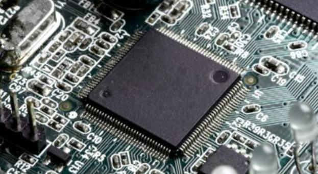
(3) component layout
Component layout and wiring have a great impact on product life, stability, electromagnetic compatibility, should pay special attention to the place. Generally speaking, there should be the following principles:
(4) Placing sequence
First place components related to the structure in fixed positions, such as power sockets, indicators, switches, connectors, etc., and then use the LOCK function of the software to lock them, so that they will not be moved by mistake in the future. Then place the special components and large components on the line, such as heating components, transformers, IC, etc. Finally place the gadget.
(5) Pay attention to heat dissipation
Component layout should pay special attention to heat dissipation. For high-power circuits, those heating components such as power tubes, transformers and so on should be placed as far as possible to the side of the distributed layout, easy to heat distribution, do not concentrate in one place, do not high capacitance too close to avoid premature aging of electrolyte.
(6) PCB wiring
Wiring principle: The knowledge of the line is very profound, everyone will have their own experience, but there are still some general principles.
(7) Adjustment and improvement
After the completion of wiring, what to do is to make some adjustments to the text, individual components, wiring and copper (this work should not be too early, otherwise it will affect the speed, and bring trouble to wiring), also in order to facilitate production, debugging, maintenance.
Copper coating usually means that a large area of copper foil is used to fill the blank area left after wiring, which can be GND copper foil or VCC copper foil (but in this case, once the short circuit is easy to burn the device, it is better to ground, unless it is necessary to increase the conduction area of the power supply to withstand larger current before connecting VCC). Ground covering usually means that two ground wires (TRAC) are wrapped around a handful of signal wires with special requirements to prevent it from being interfered with or interfered with by others.
If you use copper instead of ground wire, you must pay attention to whether the whole ground is connected, the size of the current, the flow direction and there are no special requirements, to ensure that unnecessary mistakes are reduced.
(8) Check the network
Sometimes because of misoperation or negligence caused by the drawing of the circuit board network and schematic diagram is different, then it is very necessary to check. So after the painting must not be rushed to the plate manufacturer, should do the check first, and then the follow-up work.
(9) Use simulation functions
Once you've done this, you can also do a software simulation if time permits. Especially high frequency digital circuit, so that some problems can be found in advance, greatly reduce the debugging workload in the future.


Достаточно загрузить файлы Gerber, BOM и проектные документы, и команда KINGFORD предоставит полное предложение в течение 24 часов.