How to do electromagnetic compatibility design in PCB design and wiring?
How to do electromagnetic compatibility design :1. Suitable wire width,2. Key points of component wiring,3. Wiring rules for high frequency and high speed signals


How to do electromagnetic compatibility design :1. Suitable wire width,2. Key points of component wiring,3. Wiring rules for high frequency and high speed signals
Printed Circuit Board Quality Standards and Performance Specifications Series Manual. Includes the quality standards and performance specifications set by the Printed Circuit Board Association of America for all printed circuit boards.
Many customers will require the production of halogen-free board, halogen-free board is an environmentally friendly material, halogen-free circuit board is used by the substrate is processed with halogen-free raw materials.
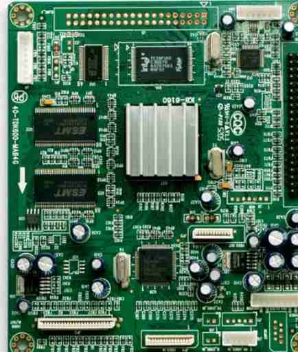
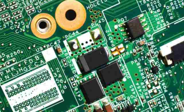
In the study, it is found that PCB design mainly has four aspects of interference: power supply noise, transmission line interference, coupling and electromagnetic interference
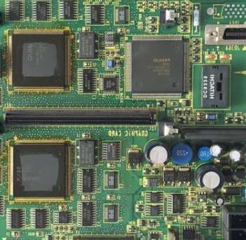
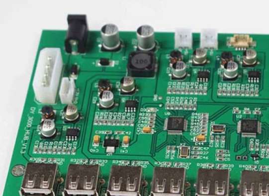
The public power cables and ground cables on the two-sided SMB should be placed near the edge of the SMB and on both sides of the SMB. The power layer and ground cable layer can be installed at the inner layer of the multi-layer SMB, and the cables, power
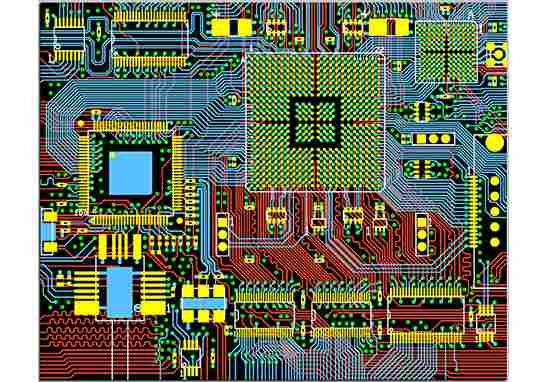
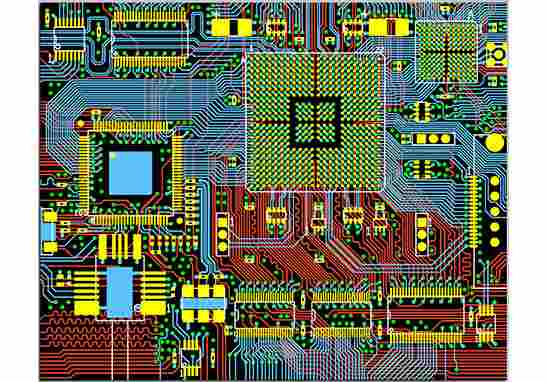
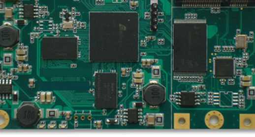
PCB layout skills: 1, arrange the position of each functional circuit unit according to the circuit flow, so that the layout is convenient for signal flow, and make the signal as far as possible to maintain the same direction, 2, the core components of ea
Common mistakes in PCB design process are summarized as follows: 1. Pad overlap; 2. Non-standard use of graphic layer; 3. Characters unreasonable, 4. Single side pad set aperture, 5. Use filler block to draw pad, 6. The electric stratum is designed with b
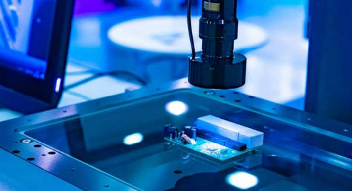
Intercept the defective devices before welding to avoid the increase of maintenance cost and scrap risk after the defective mounting devices enter reflow welding.
It mainly includes color ring resistor, carbon film resistor, cement resistor, thermistor, varistor, resistor row, variable resistor
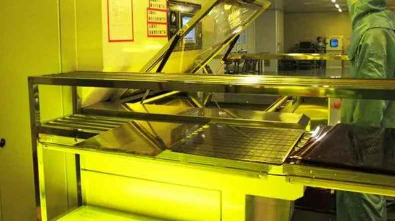
For such a small print, the press must be able to provide an excellent solution to achieve maximum coplanicity between the substrate and the steel mesh.
How to cleverly design multiple circuits of the same circuit structure quickly: 1. Design code segments (code segments), 2. Equipment Table, 3. Multi-channel design method (Multi-channel)
PCB design differential wiring operation skills: 1, activate the wiring instruction, 2, support single line Mode, 3, in the layout of small space position differential wiring, can switch to the Neck Mode, 4, according to the wiring needs to select the app


