
Контрактное производство электроники под ключ в Китае
Шэньчжэнь, район Баоань, улица Фуюн, улица Фуцяо, район 3, промышленный парк Лонгхуй 6

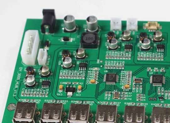
Shenzhen kingford is a professional PCB design company engaged in electronic products layout layout design, mainly undertake multi-layer, high density PCB design and circuit board design proofing business. Next, I will introduce common mistakes in PCB design.
Common mistakes are summarized in PCB design process
1. Pad overlap
▪ Caused heavy holes, during drilling because of multiple drilling in one place resulting in broken drill and hole damage.
▪ In the multilayer board, there are both connecting plates and isolating plates in the same position, and the board has been shown to have isolated connection errors.
2. The use of graphics layer is not standard
▪ Unconventional design, such as component surface design on the Bottom layer and welding surface design on the TOP layer, leads to misunderstandings.
▪ There is a lot of design junk on all levels, such as broken wires, useless borders, labels, etc.
3. Incorrect characters
▪ Character covering SMD pads, inconvenient PCB on-off testing and component welding;
▪ Small characters, resulting in screen printing difficulties, too large characters overlap each other, difficult to distinguish, the font is not. 40mil.
4. Set the aperture of single side pad
▪ Single side pad is generally not drilled, its aperture should be designed to be zero, otherwise the hole coordinates will appear in this position when drilling data is generated. Such as drilling should be special description;
▪ If the single-side pad needs to be drilled, but the aperture is not designed, the pad will be treated as SMT pad by the software during the output of electrical and stratigraphic data, and the inner layer will lose the isolation pad.
5. Paint the pad with a filler block
Although it could pass DRC inspection, welding resistance data could not be directly generated during machining, and the pad covered with solder resistance could not be welded.
6. The electric stratum has both the heat dissipation plate and the signal line. The positive and negative images are designed together, causing an error.
7. Large area grid spacing is too small
Gridline spacing < 0.3mm, PCB manufacturing process, the graphic transfer process after development, resulting in broken film resulting in line break. Improve the difficulty of processing.
8. The graphic is too close to the frame
The spacing should be at least 0.2mm or above (0.35mm or above at V-cut), otherwise the copper foil warping and flux resistance will fall off when the shape is processed. Affect the appearance quality (including the copper inner layer of multilayer board).
9. The outline frame design is not clear
Many layers are designed with a frame, and do not coincide, resulting in PCB manufacturers are difficult to judge which line molding, the standard frame should be designed in the mechanical layer or BOARD layer, the internal hollowed out part to be clear.
10. Uneven graphic design
Cause pattern plating, current distribution is not uniform, affect the coating uniform, even cause warping.
11. Abnormity hole short
The length/width of special-shaped holes should be > 2:1, width > 1.0mm, otherwise the CNC drilling machine can not process.
12. No milling contour positioning hole is designed
Design at least 2 diameters > in PCB board if possible; 1.5mm positioning hole.
13. Aperture marks are not clear
▪ Aperture labeling should be in metric system as far as possible, and in increments of 0.05.
▪ Merge possible apertures into one reservoir area.
▪ Whether the tolerances for metallized holes and special holes (e.g. crimped holes) are clearly marked.
14. The inner wiring of multilayer board is unreasonable
▪ Put the cooling pad on the isolation belt. After drilling, it is easy to fail to connect.
▪ The design of the isolation belt is notched and easy to misunderstand.
▪ The isolation belt design is too narrow to accurately judge the network
15. Design problem of buried blind hole plate
Significance of designing buried blind hole plate:
▪ Increase the density of multilayer panels by more than 30%, reduce the number of layers and reduce the size b. Improved PCB performance, especially control of characteristic impedance (wire shortening, aperture reduction);
▪ Improve PCB design freedom;
▪ Reduce raw materials and costs, which is conducive to environmental protection.
Shenzhen kingford PCB design capability
Maximum signal design rate: 10Gbps CML differential signal;
Maximum number of PCB design layers: 40;
Minimum line width: 2.4mil;
Minimum line spacing: 2.4mil;
Minimum BGA PIN spacing: 0.4mm;
Minimum mechanical hole diameter: 6mil;
Minimum laser drilling diameter: 4mil;
Maximum number of pins:; 63000 +
Maximum number of components: 3600;
Maximum number of BGA: 48+.
PCB design service process
1. The customer provides schematic diagram to consult PCB design;
2. Evaluate quotation according to schematic diagram and customer design requirements;
3. The customer confirms the quotation, signs the contract and pays the project deposit;
4. Received advance payment and arranged engineer design;
5. After the design is completed, provide the screenshot of the document to the customer for confirmation;
6. The customer confirmed OK, settled the balance, and provided PCB design materials.

Layout rules for PCB design
2023-03-14


Достаточно загрузить файлы Gerber, BOM и проектные документы, и команда KINGFORD предоставит полное предложение в течение 24 часов.