
Контрактное производство электроники под ключ в Китае
Шэньчжэнь, район Баоань, улица Фуюн, улица Фуцяо, район 3, промышленный парк Лонгхуй 6

With its expertise, Christian Koenen's Application Center has made a significant contribution to the technological development of board mounting and electronic manufacturing processes. The center acts as a collaborative platform to work with customers to develop the best solutions for demanding requirements. The center is equipped with a clean room. These are the basic preconditions to ensure that the process conditions can reliably maintain the best quality.
Together, Koh Young, Heraeus, ASYS and Christian Koenen conducted a series of experiments in which a PCB was printed 10 times without the use of solder resistance, and the bottom of the PCB was never cleaned during the printing process
.
Printing quality is tested directly with Koh Young Meister S solder paste testing equipment. About 1000 holes were used for the statistical steel mesh, and the results were verified using microscopes and laser scanners. These PCBSwere neither mounted nor printed. These tests were conducted under actual manufacturing conditions using commercially available components and materials.
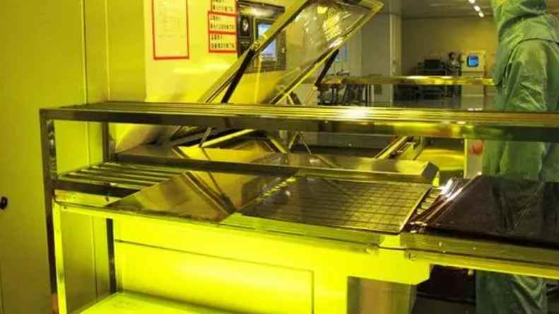
The systems and materials used include: ASYS SMD line consisting of EKRA SERIO 5000 press with transport and handling modules; Heraeus LED131 (type 6) and LED100 (type 7) Mini LED solder paste; CK Nanovate™ Nickel Mesh Plate with Plasma Treatment; And Koh Young's Meister S SPI system.

Mini LED printing test environment in Christian Koenen.
Superfine tin paste
For the miniaturized Mini LED pad geometry, a special paste with a particle smaller than 15 µl is required to obtain a reliable paste for this application.
With steel mesh thickness between 15 and 30 µl and aperture less than 80 µl, these particles reliably reduce potential poor printing, such as large fluctuations in solder paste volume or solder paste printing.
In the study described here, powders No. 6 and No. 7 were used, manufactured by the patented Welco® process. In this process, the solder alloy is first heated above its melting point range in a thermally stable dispersing medium. A special rotor-stator process is used to produce uniform solder particles after melting.
After cooling, a solder paste with a very fine particle distribution range is obtained, in this case, powder No. 6 (5 to 15 µ) and powder No. 7 (2 to 11 µ) solder paste. It is characterized by a particularly good sphericity (aspect ratio of about 1) and smooth surface.
These solder parameters help ensure excellent initial printing capability and long-term printing stability, which is particularly important for the advancement of Mini LED assembly technology.
Heraeus has developed an optimized NC flux formulation family (LED131/LED100) for these LED applications, designed to ensure excellent printability and necessary weldability. Due to the smaller particles, the surface area of the solder paste sphere is greatly increased (higher degree of oxidation), so a reliable activation design must first be designed.
The aim is to enable all participating connection parts (especially the Mini LED and substrate) to achieve good wetting and to achieve low voidage to maintain the necessary insulation value (SIR) of the remaining flux residue.
In addition to these considerations and standard requirements for solder paste (such as low slump and low ball formation), special attention should be paid to ensuring that the solder paste is sufficiently viscous prior to reflow soldering. This keeps the Mini LED particles and their apparently minimized connection areas in place before reflow soldering.
Steel mesh
The material of CK nickel steel mesh has been improved in recent years by Christian Koenen's team. Hence the CK Nanovate nickel steel mesh. The introduction of this superalloy makes it possible to cut nickel with lasers without forming micro-cracks. This material combines the advantages of nickel and stainless steel mesh and solves its disadvantages.
The company can produce steel mesh series up to 15 µl thickness. The team used steel mesh with a thickness of 15 to 30 µl to evaluate different areas and filling rates.
To get representative results, the team decided to go with 45 x 45 µl, 60 x 60 µl, and 80 x 80 µl, although there are different sizes of Mini leds available.
Printability of the holes is further improved because the underside of the mesh and the inner wall of the holes are Plasma 3.0 coated. The coating reduces the adhesion between the solder paste and the steel mesh, resulting in better release from the pores, and reduces volume dispersion between the grooves and between subsequent printing cycles.
Koh Young's Meister S SPI device.
Printing system
Modern steel mesh presses must be highly flexible and, like the EKRA SERIO 5000, can dynamically meet changing requirements. The key factor to determine solder paste printing is the flatness of the substrate and its coplanar property with the steel mesh.
Typically, Mini LED substrates are only a few tenths of a millimeter thin, making them prone to bending.
EKRA's advanced printing heads are specifically designed for ultra-fine spacing applications. The pressure of the scraper is precisely printed within a narrow tolerance.
All relevant printing parameters are continuously transmitted to the Koh Young KPO detection solution via the EKRA high-end closed-loop interface, where they are recorded and automatically optimized. Scrapers and strippers can be fine-tuned for applications such as highly miniaturized Mini leds without any adjustment by the operator.
In automatic optical detection, there is always a compromise between detection speed and measurement accuracy. Dealing with Mini leds with SPI system also involves pixel size issues. In this case, this means that the smaller the LED, the higher the resolution of the display. A repeatable measurement requires about 100 pixels of information. Then, you can quickly infer from the size of the pattern.
Another important aspect is Z-axis resolution. The optical measurement system evaluates the grayscale phase shift between individual pixels. The light is projected into the camera field from both sides at a definite Angle. The projection Angle and pixel size are related to the Z-axis height resolution.
The Meister S SPI system is designed to meet these requirements. In this study, the pixel size was reduced to 5 μs and the projection Angle was minimized. Although this results in a height measurement range halved from the standard SPI, high accuracy at low altitudes is a must for specific applications of the Meister S system. In addition, the Plus version of the Meister device is specially optimized for reflective surfaces.
The study reveals the physical limits of optical inspection. To meet future demands, Koh Young is already designing a new camera system with a resolution of up to 3.5μs.
For such a small print, the press must be able to provide an excellent solution to achieve maximum coplanicity between the substrate and the steel mesh.
Pre-processing /THT/ hand welding process
2023-03-13


Достаточно загрузить файлы Gerber, BOM и проектные документы, и команда KINGFORD предоставит полное предложение в течение 24 часов.