
Контрактное производство электроники под ключ в Китае
Шэньчжэнь, район Баоань, улица Фуюн, улица Фуцяо, район 3, промышленный парк Лонгхуй 6

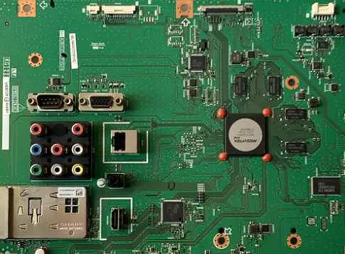
Shenzhen kingford has a PCB design team with an average of more than 10 years of working experience, who can skillfully use the mainstream PCB design software in the market, professional and efficient communication to ensure the progress of PCB design, and help you to seize the market opportunity earlier! Next, Shenzhen PCB design company - Shenzhen kingford to introduce the PCB process design requirements in detail.
1. Add test points
1. In order to meet various test requirements, it is generally required that each network has at least one test point for the probe to contact;
2. Select the type of test point. The recommended priority is PAD > component welding hole > signal passthrough hole;
3. The size of the pad at the test point shall not be less than 26mil (0.65mm), and the minimum distance between the center of the two separate test points shall be 50mil (1.25mm);
4. For boards requiring ICT testing, two 3mm diameter nonmetallic holes should be designed on the diagonal of PCB for ICT testing and positioning.
Two, optical anchor point
In order to meet the requirements of patch component production, each PCB board shall have at least two Fiducial marks for correcting the deviation of the X or Y axis of the component. The principle of their placement is:
1. There should be at least two or more optical registration points on the PCB board, among which any two registration points should be distributed diagonally, and the other asymmetric registration point should be placed outside the diagonal position;
2. If no working edge is added outside the PCB board, the optical positioning point shall be more than 3mm away from each board edge;
3. The optical calibration points on the same PCB board shall be of the same specification, and the minimum diameter of the calibration points shall be 1mm, and the maximum diameter shall not exceed 1.5mm;
4. The optical positioning point should have the highest contrast with the PCB substrate for the best effect, so as to be accurately identified;
5. If the plate is needed, ensure that there is at least one optical anchor point on each board;
6. Similar similar points (which may also be components, or regional graphics formed by signal holes and copper application) are prohibited within 15mm around the optical anchor point.
3, add working edge
1. When the size of PCB board is large enough and there are no components placed within 3mm of the two long sides of the board, the 3mm wide board can be used as the working edge;
2. When the PCB board size is not large enough and the distance between the components in the board and the edge of the board cannot meet the requirement of 3mm, it is necessary to add an 8mm board on the outside of the two long sides of the PCB board as the working edge.
4, film file output
According to the situation of domestic suppliers, usually the board film file is in RS-274X format.
5, the rules of Mosaic
1. When the molding size of PCB board is less than 50*50mm, it must be pieced out;
2. PCB plate size should be less than 250*350mm;
3. PCB board components must be at least 1mm away from the V-CUT line;
4. For the number of patchwork, the sum of the front and back patches is about 600;
5. If V-CUT is used in production, when "L" type PCB board is assembled, 11*5mm slot holes must be set aside between the two boards to stop the knife;
6. In addition to the above rules, when assembling boards, it is also necessary to calculate the utilization rate of materials according to the size and specification of PCB manufacturer's substrate, so as to improve the utilization rate to determine the number of assembling boards and control the cost.
Vi. Information annotation in the board
1. For PCB dimension marking, the exact outline size of PCB is generally marked in the drilling layer, and the closed dimension marking cannot be formed. At the same time to indicate the size and number of all holes, and indicate whether the type of hole is metallized holes;
2. Each layer of PCB should have sequence marks indicating the sequence of layers. Sequence marks should be arranged in sequence.
3. The silk screen layer of the PCB board should be marked with the bit number of the marking component, and the marked direction can only be two directions in the same PCB board, and can not be placed arbitrarily;
4. If there is a dangerous high-voltage circuit in the board, mark the high-voltage warning sign in the high-voltage area;

If there is a dangerous high-voltage circuit in the board, mark the high-voltage warning sign in the high-voltage area
5. If the PCB board is a lead-free process, the lead-free process symbol is usually marked on the board in order to distinguish it from the PCB with lead;
If the PCB board is a lead-free process, the lead-free process symbol is usually labeled on the board to distinguish it from a PCB with lead
Finally, it should be noted that PCB information labeling requirements are not mandatory, but according to the previous research and development experience, the standardization of design process has a profound impact on the research and development efficiency, research and development cost, and even on the reliability of products. Therefore, Shenzhen Honglijieh strongly recommends that we strictly follow the standardized research and development process and develop good design habits. The future will determine the height an engineer can reach.
2. What are the main contents of incoming material inspection for SMT patch processing?
Next, we will introduce the main content of incoming material inspection for SMT patch processing.
First, what is the SMT patch processing incoming material inspection?
Incoming material inspection before SMT patch processing is the primary condition to ensure the quality of SMT patch. The quality of components, PCB board and SMT patch processing materials directly affects the quality of PCB patch. Therefore, there should be strict incoming material inspection and management system for electrical performance parameters of components, weldability of welding ends and pins, producible design of PCB board and weldability of welding pad, quality of SMT SMT processing materials such as solder paste, patch adhesive, rod solder, flux and cleaning agent. The quality problems of components, PCB board and SMT patch processing materials are difficult or even impossible to solve in the later process.
2. Incoming inspection of SMT patch processing components
The main test items of the components include: weldability, pin coplanar and serviceability, which shall be inspected by the incoming materials inspection department. The weldability of components can be tested by holding the components with stainless steel tweezers and dipping them into a tin pot at 235±5℃ or 230±5℃, and taking them out at 2±0.2s or 3±0.5s. Check the solder end under a 20-fold microscope, and the solder end of components should be more than 90% tin.
The patch processing workshop can do the following appearance inspection:
1. Visually or with a magnifying glass, check whether the welding end or pin surface of the component is oxidized or has any pollutants.
2. The nominal values, specifications, models, accuracy and dimensions of the components shall be consistent with the technical requirements of the products.
3. The pins of SOT and SOIC cannot be deformed. For the multi-lead QFP devices with lead spacing less than 0.65mm, the coplanicity of the pins should be less than 0.1mm(which can be detected by the optical mounting machine).
4. For products required to be cleaned, the marks of components shall not fall off after cleaning, and the performance and reliability of components shall not be affected (visual inspection after cleaning).
Three, PCB board (PCB) incoming material inspection
1. PCB welding pad graphics and dimensions, welding resistance film, screen, through hole Settings should meet the design requirements of SMT PCB board. (For example: check whether the welding distance is reasonable, whether the screen is printed on the pad, whether the passthrough hole is done on the pad, etc.).
2. The overall size of PCB should be consistent, and the overall size, positioning hole and reference mark of PCB should meet the requirements of production line equipment.
3. Permissible warping size of PCB:
1) Upward/convex surface: maximum length 0.2mm/5Omm maximum length 0.5mm/ length direction of the whole PCB.
2) Downward/concave: maximum length 0.2mm/5Omm maximum length 1.5mm/ length direction of the whole PCB.
4. Check whether the PCB is contaminated or damp.
Shenzhen kingford circuit board design capability
Maximum signal design rate: 10Gbps CML differential signal;
Maximum number of PCB design layers: 40;
Minimum line width: 2.4mil;
Minimum line spacing: 2.4mil;
Minimum BGA PIN spacing: 0.4mm;
Minimum mechanical hole diameter: 6mil;
Minimum laser drilling diameter: 4mil;
Maximum number of pins:; 63000 +
Maximum number of components: 3600;
Maximum number of BGA: 48+.
PCB design service process
1. The customer provides schematic diagram to consult PCB design;
2. Evaluate quotation according to schematic diagram and customer design requirements;
3. The customer confirms the quotation, signs the contract and pays the project deposit;
4. Received advance payment and arranged engineer design;
5. After the design is completed, provide the screenshot of the document to the customer for confirmation;
6. The customer confirmed OK, settled the balance, and provided PCB design materials.


Достаточно загрузить файлы Gerber, BOM и проектные документы, и команда KINGFORD предоставит полное предложение в течение 24 часов.