
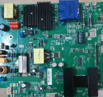
Контрактное производство электроники под ключ в Китае
Шэньчжэнь, район Баоань, улица Фуюн, улица Фуцяо, район 3, промышленный парк Лонгхуй 6

Before starting the wiring, the PCB design should be carefully analyzed and the tool software should be carefully set up, which will make the PCB design more in line with the requirements. Next, Shenzhen kingford, a PCB design company in Shenzhen, will introduce the preliminary work to be done before PCB design.
The preliminary work needs to be done before PCB design
1. Determine the number of PCB layers
The size of the circuit board and the number of wiring layers need to be determined at the early stage of PCB design. The number of wiring layers and STack-up mode will directly affect the wiring and impedance of printed lines. The size of the board helps to determine the layering pattern and the width of the printed line to achieve the desired PCB design effect. At present, the cost difference between multilayer boards is very small, and it is better to use more circuit layers and make the copper evenly distributed at the beginning of PCB design.
2. PCB design rules and restrictions
To successfully complete the wiring task, wiring tools need to work within the correct rules and constraints. All signal lines with special requirements should be classified. Each signal class should have a priority. The higher the priority, the stricter the rules. The rules involve the width of printed lines, the maximum number of holes through, parallelism, the interaction between signal lines, and the limits of layers. These rules have a great impact on the performance of wiring tools.
Careful consideration of PCB design requirements is an important step in successful wiring.
During optimal assembly, manufacturable PCB design (DFM) rules restrict component layout. If the assembly department allows the components to move, the circuit can be optimized for automatic wiring. The rules and constraints defined affect the layout PCB design. The automatic wiring tool considers only one signal at a time. By setting the constraints of the wiring and setting the layers of the deployable signal lines, the wiring tool can be enabled to complete the wiring as envisioned by the PCB designer.
For example, for the layout of the power line: (1) In the PCB layout, the power decoupling circuit PCB should be designed near the relevant circuits, rather than placed in the power supply part, otherwise it will not only affect the bypass effect, but also flow pulsating current on the power line and ground wire, causing interference; (2) For the power supply direction inside the circuit, power supply should be taken from the last stage to the forward stage, and the power filter capacitor of this part is arranged near the last stage; (3) For some main current channels, such as in the debugging and detection process to disconnect or measure the current, in the layout should be arranged on the printed wire current gap.
In addition, we should pay attention to the regulated power supply in the layout, as far as possible arranged in a separate printed board. When the power supply and circuit are used together in the printed board, in the layout, the voltage regulator should avoid mixing the power supply and circuit components or making the power supply and circuit common ground.

Because this wiring is not only prone to interference, but also unable to disconnect the load during maintenance, only part of the printed wire can be cut, thus damaging the printed board.
4, fan out PCB design
During the fan-out PCB design phase, each pin of the surface-mount device should have at least one through-hole so that the board can be made for inner connections, in-line testing, and circuit reprocessing when more connections are needed.
In order to maximize the efficiency of the automatic wiring tool, it is necessary to use the largest hole size and printed lines possible, with an interval of 50mil being ideal. Use the hole type that maximizes the number of routing paths. After careful consideration and prediction, PCB design for online circuit testing can be carried out at the early stage of PCB design and realized later in the production process.
The type of through-hole fan-out is determined based on the wiring path and online circuit testing. Power supply and grounding also affect the wiring and fan-out PCB design.
5, manual wiring and key signal processing
Manual wiring is an important process in PCB design now and in the future. Using manual wiring helps automatic wiring tools to complete the wiring work.
By manually routing and fixing the selected net, a path can be formed for automatic routing.
First of all, key signals can be wired manually or combined with automatic wiring tools. After the wiring is completed, the relevant engineering and technical personnel will check the signal wiring. After the check is passed, the wires will be fixed, and then the rest of the signals will be automatically wired.
Because of the existence of impedance in ground wire, common impedance interference will be brought to the circuit. Therefore, when wiring, do not connect any point with ground symbol, which may produce harmful coupling, affect the work of the circuit.
At higher frequencies, the inductive reactance of the wire will be several orders of magnitude greater than the resistance of the wire itself. At this time, even if only a small high frequency current flows through the wire, there will be a certain high frequency voltage drop. Therefore, for high frequency circuits, the PCB layout is as compact as possible so that the printed wires are as short as possible.
There are mutual inductance and capacitance between printed wires. When the working frequency is large, it will cause interference to other parts, which is called parasitic coupling interference. The suppression methods can be adopted: ① shorten the signal routing between levels as far as possible; ② Arrange all levels of circuits according to the order of signals to avoid each level of signal lines crossing each other; ③ The wires of the adjacent two panels should be vertical or cross, not parallel; (4) When signal wires are arranged in parallel in the board, these wires should be separated as far as possible by a certain distance, or separated from the ground line and the power line to achieve the purpose of shielding.
6. Automatic wiring
For the wiring of key signals, it is necessary to consider the control of some electrical parameters during wiring, such as reducing the distributed inductance, etc. After understanding the input parameters of automatic wiring tools and the influence of input parameters on wiring, the quality of automatic wiring can be guaranteed to a certain extent.
General rules should be applied in the automatic wiring of signals. The wiring tool can automatically route a given signal according to the engineer's PCB design ideas by limiting the layers to be used and the number of holes to be used by setting limits and prohibited wiring zones. After the constraints are set and the rules created are applied, the automatic wiring will achieve similar results as expected. After a portion of the PCB is designed, it will be fixed to prevent it from being affected by the subsequent wiring process.
The amount of wiring depends on the complexity of the circuit and the number of common rules defined. Today's automatic wiring tools are very powerful and usually complete 100% of the wiring. However, when the automatic wiring tool does not complete all signal wiring, the remaining signals need to be routed manually.
7. Arrangement of wiring
For some signals with few constraints, the length of wiring is very long. At this time, we can first judge which wiring is reasonable and which wiring is not reasonable, and then shorten the length of signal wiring and reduce the number of holes by manual editing.
Shenzhen kingford PCB design capability:
Maximum signal design rate: 10Gbps CML differential signal;
Maximum number of PCB design layers: 40;
Minimum line width: 2.4mil;
Minimum line spacing: 2.4mil;
Minimum BGA PIN spacing: 0.4mm;
Minimum mechanical hole diameter: 6mil;
Minimum laser drilling diameter: 4mil;
Maximum number of pins:; 63000 +
Maximum number of components: 3600;
Maximum number of BGA: 48+.
PCB design service process
1. The customer provides schematic diagram to consult PCB design;
2. Evaluate quotation according to schematic diagram and customer design requirements;
3. The customer confirms the quotation, signs the contract and pays the project deposit;
4. Received advance payment and arranged engineer design;
5. After the design is completed, provide the screenshot of the document to the customer for confirmation;
6. The customer confirmed OK, settled the balance, and provided PCB design materials.
Circuit board design manufacturers
2023-03-16


Достаточно загрузить файлы Gerber, BOM и проектные документы, и команда KINGFORD предоставит полное предложение в течение 24 часов.