
Контрактное производство электроники под ключ в Китае
Шэньчжэнь, район Баоань, улица Фуюн, улица Фуцяо, район 3, промышленный парк Лонгхуй 6

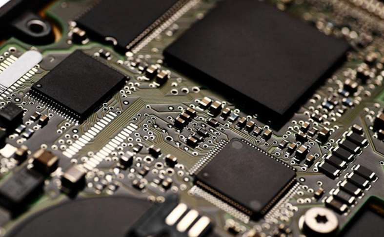
With the development of communication technology, wireless high-frequency circuit technology is used more and more widely. The performance index of the high-frequency circuit directly affects the quality of the whole product. The layout and wiring of components can maximize the performance index of the circuit and achieve the design purpose of anti-interference.
Because the surface patch generally adopts infrared furnace heat flow welding to realize the welding of components, so the layout of components affects the quality of solder joints, and then affects the yield of products.
In addition to considering the layout of ordinary PCB design, we also consider how to reduce the mutual interference between each part of the high-frequency circuit, how to reduce the interference of the circuit itself to other circuits and the anti-interference ability of the circuit itself.
The effect of high frequency circuit not only depends on the performance of the High Frequency Circuit Board itself, but also depends on the interaction with the CPU processing board. Therefore, reasonable layout in PCB design. The general principle of layout is that the components should be arranged in the same direction as far as possible. By choosing the direction of PCB into the molten tin system, the phenomenon of poor welding can be reduced or even avoided.
Details in the layout:
(1) First determine the position with other PCB board or system interface components on the PCB board, must pay attention to the coordination between the interface components (Canadian dollar device direction, etc.);
(2) Because the volume of handheld products are small, the components are arranged very compact, so for the larger volume of components, must give priority to determine the corresponding position, and consider the problem of coordination between each other;
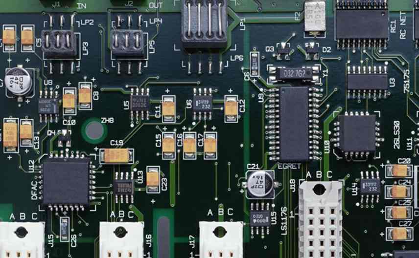
(3) Carefully analyze the circuit structure, the circuit for block processing (plus high frequency amplifier circuit, mixing circuit and demodulation circuit, etc.), as far as possible strong signal and weak signal separated, the digital signal circuit and analog signal circuit separated, complete the same function of the circuit should be arranged in a certain range, so as to reduce the signal loop area; The filtering network of each part of the circuit must be connected nearby, which can not only reduce the radiation height, but also reduce the probability of interference and improve the anti-interference ability of the circuit.
(4) Unit circuits are grouped according to their sensitivity to electromagnetic compatibility in use.
Step 2: Wiring
After basically completing the layout of components, wiring can begin. The basic principle of wiring is: in the case of assembly density permit, as far as possible to choose low-density wiring design, and signal routing as far as possible the thickness of the same, conducive to impedance matching.
In the design of high frequency circuit PCB, the strike, width and line spacing of signal lines are considered. wiring, Keep all the cables 2 mm away from the PCB board frame to avoid cable breakage or hidden dangers during PCB fabrication.
The power cord should be as wide as possible to reduce loop resistance, and the direction of the power cord and ground wire should be consistent with the direction of data transmission to improve anti-interference ability; The signal lines should be as short as possible and the number of holes should be minimized; The wires between components should be as short as possible to reduce the distribution parameters and electromagnetic interference between each other; Incompatible signal cables should be kept away from each other as far as possible, and parallel cables should be avoided as far as possible. Signal cables on both sides should be perpendicular to each other; Wiring in the need of the corner should be 135° Angle is appropriate, avoid turning a right Angle.


Достаточно загрузить файлы Gerber, BOM и проектные документы, и команда KINGFORD предоставит полное предложение в течение 24 часов.