
Контрактное производство электроники под ключ в Китае
Шэньчжэнь, район Баоань, улица Фуюн, улица Фуцяо, район 3, промышленный парк Лонгхуй 6

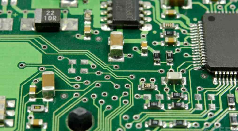
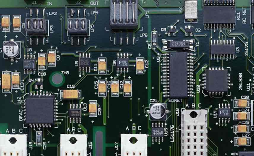
In our daily life, almost every kind of electronic equipment we come into contact with will appear printed circuit boards. If there are electronic parts in a certain kind of equipment, they are all embedded on PCB of different sizes. In order to obtain the best performance of electronic circuits, the Layout of components and wires are very important, and wiring as the top priority of PCB design process, which will directly affect the performance of PCB board. Although many advanced EDA tools now provide automatic wiring function, and also quite intelligent, but automatic wiring can not guarantee a hundred percent of the cloth through rate.
The rate of automatic wiring depends on good layout, wiring rules can be set in advance, including the number of bending times, the number of through holes, the number of steps and so on. Generally, first explore the cloth warp, quickly connect the short line, and then labyrinth wiring, first to cloth the wire for global wiring path optimization, it can be disconnected according to the need of the cloth line. And try rewiring to improve the overall effect.
PCB wiring and classification is the same reason, single-sided wiring, double-sided wiring and multi-layer wiring, and there are two ways of wiring, automatic wiring and interactive wiring, before automatic wiring, you can use interactive prior to the requirements of strict line wiring, input and output side line should avoid adjacent parallel, so as to avoid reflection interference. Grounding should be added when necessary, two adjacent layers of wiring should be vertical to each other, parallel easy to produce parasitic coupling.
In PCB wiring, it is inevitable to turn the wire. When the right Angle of the wire appears, extra parasitic capacitance and inductance will be generated at the corner. The corners should be designed at sharp angles and right angles to avoid unnecessary radiation.
Secondly, the line should be streamlined, as short as possible, as little as possible to turn, and strive for simple and clear lines, especially in the high-frequency circuit, of course, in order to achieve impedance matching and the need for special extension of the line is the exception, such as snake line, etc. The width of copper wire should be designed based on the current it can carry. The current-carrying capacity of copper wire depends on the following factors: wire width, wire thickness (copper platinum thickness), allowable temperature rise, etc. The following table gives the relationship between the width of copper wire, wire area and conducting current (military standards). The width of wire can be properly considered according to this basic relationship.
In addition, the minimum width of PCB board wire is mainly determined by the adhesion strength between the wire and the insulating substrate and the current flowing through them. Input and output wires should be as close to each other as possible. It is better to add ground wire to avoid feedback coupling. The minimum distance between wires is mainly determined by the insulation resistance and breakdown voltage between wires in the worst case. For integrated circuits, especially digital circuits, as long as the process allows, the spacing can be as small as 5 ~ 8 mm. Printed wire bends in a circular arc, and right or included angles will affect the electrical performance in high frequency circuits. In addition, try to avoid using a large area of copper foil, otherwise, when heated for a long time, it is easy to occur copper foil expansion and shedding phenomenon. When a large area of copper foil must be used, it is best to use a grid, which is conducive to the exclusion of volatile gases generated by the heat of the adhesive between the copper foil and the substrate.
After the wiring design is completed, it is necessary to carefully check whether the wiring design conforms to the rules formulated by the designer, and also confirm whether the rules formulated meet the requirements of the printed board production process. General check: wire to wire, wire and component pad, wire and through hole, component pad and through hole, whether the distance between through hole and through hole is reasonable, and whether the Production requirements are met. Are optimal measures taken for critical signal lines, such as minimum length, protected lines, and clearly separated input and output lines.
High frequency PCB board
2023-03-22


Достаточно загрузить файлы Gerber, BOM и проектные документы, и команда KINGFORD предоставит полное предложение в течение 24 часов.