
Контрактное производство электроники под ключ в Китае
Шэньчжэнь, район Баоань, улица Фуюн, улица Фуцяо, район 3, промышленный парк Лонгхуй 6


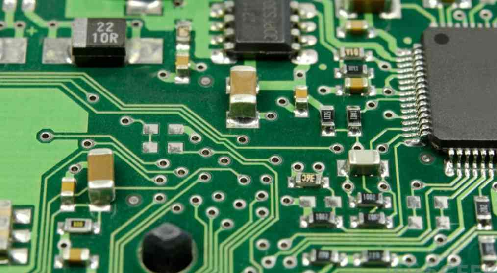
We say that PCB board is to design the schematic into a real PCB board, please don't look down on this process, there are a lot of workable things in principle in the project is difficult to achieve, or others can achieve things that some people can not achieve, so it is not difficult to do a good PCB board, but to do a good PCB board is not an easy thing.
The two major difficulties in the field of microelectronics are the processing of high-frequency signals and weak signals, in this respect PCB production level is particularly important, the same principle design, the same components, different people produced PCB will have different results, so how to make a good PCB board? Based on our previous experience, I would like to share my views on the following aspects:
First, to clear the design objectives
When receiving a design task, it is necessary to clarify its design objectives, which are ordinary PCB board, high frequency PCB board, small signal processing PCB board or both high frequency and small signal processing PCB board. If it is an ordinary PCB board, as long as the layout and wiring are reasonable and neat, and the mechanical size is accurate, such as medium load line and long line, It is necessary to use certain means to deal with, reduce the load, long line to strengthen the drive, is to prevent long line reflection.
When there are more than 40MHz signal lines on the board, special consideration should be given to these signal lines, such as cross-talk between the lines and other issues. If the frequency is higher, there will be a strict limit on the length of the wiring. According to the network theory of distributed parameters, the interaction between the high-speed circuit and its wire is the decisive factor, which cannot be ignored in the system design. With the increase of the gate transmission speed, the opposition on the signal line will increase correspondingly, and the crosstalk between adjacent signal lines will increase in direct proportion. Usually, the power consumption and heat dissipation of high-speed circuits are also large, so sufficient attention should be paid to the high-speed PCB.
When there is a weak signal of millivolt level or even microvolt level on the board, special attention is needed for these signal lines. Small signals are too weak and very susceptible to interference from other strong signals. Shielding measures are often necessary, otherwise the signal-to-noise ratio will be greatly reduced. So that useful signals are drowned out by noise and cannot be effectively extracted.
The commissioning of the board should also be considered in the design phase, the physical location of the test point, the isolation of the test point and other factors can not be ignored, because some small signals and high frequency signals can not be directly added to the probe to measure.
In addition, some other relevant factors should be considered, such as the number of layers of the board, the packaging shape of the components used, the mechanical strength of the board, etc. Before doing PCB board, to make the design of the design goal in mind.
Two, understand the function of the components of the layout and wiring requirements

We know that some special components have special requirements in the layout of wiring, such as LOTI and the analog signal amplifier used by APH. Analog signal amplifiers require stable power supply and small ripple. The analog small signal part should be far away from the power device as far as possible. On the OTI board, the small signal amplification part is also specially equipped with a shield to shield the stray electromagnetic interference. The GLINK chip used on the NTOI board uses the ECL process, the power consumption is large and the heat is severe. Special consideration is given to the heat dissipation problem in the layout. If the natural heat dissipation is used, it is necessary to put the GLINK chip in the place where the air circulation is relatively smooth, and the heat released can not constitute a big influence on other chips. If the board is equipped with a horn or other high-power devices, it is possible to cause serious pollution to the power supply, which should also cause enough attention.
3. Consideration of component layout
One factor to consider in the Layout of components is the electrical performance. Put the components with close connection together as far as possible, especially for some high-speed lines. The layout should make it as short as possible, and the power signal and small signal devices should be separated. On the premise of meeting the circuit performance, it is also necessary to consider that the components are placed neatly, beautiful, and easy to test. The mechanical size of the board and the location of the socket also need to be seriously considered.
Transmission delays on ground and interconnect lines in high-speed systems are also factors to be considered in system design. The transmission time on the signal line has a great impact on the total system speed, especially on the high-speed ECL circuit. Although the integrated circuit block itself has a high speed, the increase of delay time brought by the common interconnect on the baseboard (about 2ns delay per 30cm line length) can greatly reduce the system speed of the image shift register. Synchronous counter this kind of synchronous working part is better placed on the same piece of plug-in board, because to different plug-in board clock signal transmission delay time is not equal, may make the shift register production error, if not placed on a board, is the key place in synchronization, from the public clock source connected to each plug-in board clock line length ** equal.
Four, the consideration of wiring
With the completion of the design of OTNI and the star-shaped fiber network, there will be more boards with high speed signal lines above 100MHz to be designed in the future. Some basic concepts of high speed lines will be introduced here.
Pcb transmission line
2023-03-22


Достаточно загрузить файлы Gerber, BOM и проектные документы, и команда KINGFORD предоставит полное предложение в течение 24 часов.