
Контрактное производство электроники под ключ в Китае
Шэньчжэнь, район Баоань, улица Фуюн, улица Фуцяо, район 3, промышленный парк Лонгхуй 6

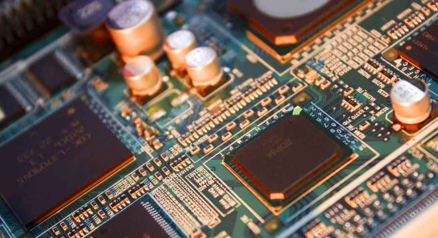
There is an old saying that PCB design is 90% layout and 10% wiring. So, what are the tips for PCB wiring?
1. Don't rely on your automatic wiring device
Almost all PCB design software includes a tool called an autocabler, but an autocabler will never replace itself in wiring and should only be used for several reasons, including:
Be precise. After all the components have been placed, you can use an auto-route to see the level of completion achieved.
Bottleneck. You can also use the auto-route to discover bottlenecks and other critical connection points that you may not have seen during component placement.
Inspiration. Use the auto wiring device as a source of inspiration to learn how to wire traces that you can't do.
In addition to the above reasons, it is recommended not to rely on automatic wiring to complete all the wiring on the PCB circuit board layout.
2. Understand the manufacturer's specifications
Before you begin laying copper wiring, call or email the customer and ask if they have any specific requirements for minimum wiring width, spacing, and the number of layers that can be handled. By knowing this information up front, you can set the wire width and spacing values in the design rules, rather than having to reroute the entire board layout.
3. Find the trace width
To determine the thickness of the line, you can use a handy line width calculator like Advanced Circuit, which will allow you to plug in the estimated current and thickness and get the line width value in exchange for the inner and outer layers.
4. Leave enough space between the tracks
Be sure to leave enough space between all the wiring and pads of the PCB layout. It is recommended to always leave a gap between 0.007 "and 0.010" between all adjacent pads on the board and the wiring.
5. Use capture grids to make your job easier
It is recommended to set the capture grid spacing to 0.050 inches during wiring. When you need to design tightly spaced connections between components, you can also set the alternate spacing to 0.025 inches.
6. Avoid using a 90-degree cable Angle
When the circuit board has a bundle of sharp right-angled turns, the outer corner of that 90-degree Angle may be etched narrower than the standard line width, resulting in a short circuit. As a solution to this problem, try using a 45 degree angular trace.
7. Leave a space between the cable and the mounting hole
When using mounting holes, always remember to leave space beyond the physical dimensions of the mounting holes to prevent them from being affected by other components and nearby marks.
8. Always create a ground cable
There must be a common ground on the PCB board because it provides the same reference point for measuring voltage for all wires. Once the grounding layer is added, simply connect all the components that need to be grounded through the through-hole.
9. Expand power supply and ground wiring
Both the power supply and ground wiring will flow more current, and if you don't make them travel wider than usual, this could eventually burn the wires and damage your device and circuit board.
10. Use through hole heat dissipation
The through-hole is ideal not only for providing electrical connections between layers, but also for transferring heat from one side of the plate.
How to avoid rework in PCB design
2023-03-17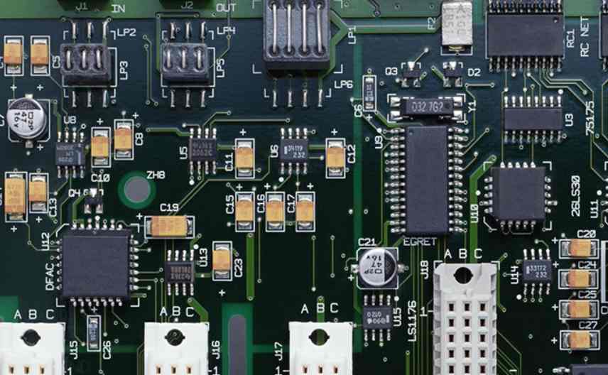


Достаточно загрузить файлы Gerber, BOM и проектные документы, и команда KINGFORD предоставит полное предложение в течение 24 часов.