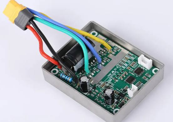
PBC self - recovery fuse selection points
Although the circuit protection device is much smaller than in the past, it is impossible to add the circuit protection device without sufficient space after the PCB design is completed.


Although the circuit protection device is much smaller than in the past, it is impossible to add the circuit protection device without sufficient space after the PCB design is completed.
As we all know, circuit protection is mainly to protect the components of electronic circuits from damage under the circumstances of overvoltage, overcurrent, surge, electromagnetic interference, and so on, and the selection of appropriate circuit protect

A tin or lead tin resist covering the top of the line extends to both sides, forming a "rim" that covers a small portion of the sensitive film underneath the "rim".

installed on the Printed Circuit Board (PCB) surface or other substrate surface, through reflow welding or immersion welding and other methods to be welded and assembled circuit installation technology.
When working, the value of Vg (that is, the voltage value of the input signal) is a fixed value, which is either high level (may fluctuate) or low level.
In order to eliminate electrostatic discharge (ESD) interference and damage to electronic equipment, it is necessary to take a variety of technical measures to prevent.

It is characterized by surface mounting of components and reflow welding technology. It has become a new generation of assembly technology for electronic products manufacturing.

On the one hand, by controlling the high level voltage applied in the grid *, there is a channel between the source and drain, and the electrons flow from the source to the drain through the channel, and the direction of the current is from the drain to t
The lines form "copper roots" on both sides after etching, and the copper roots narrow the line spacing, resulting in printed circuit boards that do not meet the requirements of Party A, and may even be rejected.

There is a little bit of short circuiting between digital and analog, but note that there is only one connection point. There are also differences on the PCB, which is determined by the system design.
It is characterized by surface mounting of components and reflow welding technology. It has become a new generation of assembly technology for electronic products manufacturing.
prepare the component library of schematic SCH and the component library of PCB. Component library can use protel (many electronic veteran birds have protel at that time


