
Контрактное производство электроники под ключ в Китае
Шэньчжэнь, район Баоань, улица Фуюн, улица Фуцяо, район 3, промышленный парк Лонгхуй 6

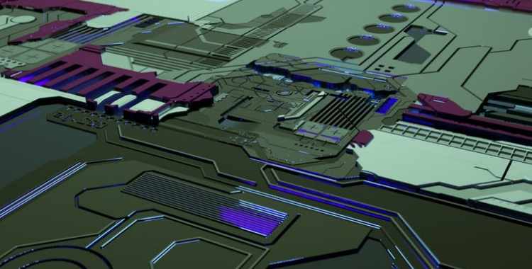
The general PCB basic design process is as follows: preliminary preparation -> PCB structure design -> PCB layout -> Wiring -> Wiring optimization and silk Screen printing -> Network and DRC check and Structure check -> Plate making.
* : Preliminary preparation.
This includes preparing component libraries and schematics. "If a worker wants to do a good job, he must first sharpen his tools." In order to make a good board, he must not only design the principle, but also draw well. Before proceeding to PCB design, * prepare the component library of schematic SCH and the component library of PCB. Component library can use protel (many electronic veteran birds have protel at that time
* II: PCB structure design.
In this step, according to the size of the circuit board and various mechanical positioning, PCB board surface is drawn in the PCB design environment, and the required connectors, keys/switches, screw holes, assembly holes and so on are placed according to the positioning requirements. And fully consider and determine the wiring area and non-wiring area (such as how much of the area around the screw hole belongs to the non-wiring area).
* Three: PCB layout.
Layout is simply putting devices on the board. At this time, if all the preparations mentioned by * are well done, the network table can be generated on the schematic diagram (Design-> Create Netlist), and then import the network table on the PCB (Design-> Load Nets). I saw the devices all piled up, and there were flying lines between the pins. Then you can lay out the device. The general layout is carried out according to the following principles:
(1) According to the electrical performance reasonable partition, generally divided into: digital circuit area (fear of interference, and interference), analog circuit area (fear of interference), power drive area (interference source);
②. Complete the circuit of the same function, should be placed as close as possible, and adjust the components to connect more concise; At the same time, adjust the relative position between the functional blocks to make the connection between the functional blocks more concise;
(3) The installation position and installation strength of the components with high quality should be considered; The heating element should be placed separately from the temperature sensitive element, and the heat convection measures should be considered if necessary;
(4) I/O driving device as close as possible to the edge of the printing plate, close to the outlet connector;
⑤. Clock generator (such as crystal oscillator or clock oscillator) should be as close to the device that uses the clock as possible;
In each integrated circuit between the power input foot and the ground, need to add a decoupling capacitor (generally use high frequency performance good * stone capacitor); When the board space is dense, a tantalum capacitor can also be added around several integrated circuits.
⑦. Relay coil to add discharge diode (1N4148 can);
⑧. Layout requirements to balance, dense and orderly, not top-heavy or heavy

-- requires special attention
When placing components, it is necessary to consider the actual size of components (occupied area and height), the relative position between components, to the electrical performance of the circuit board and the feasibility and convenience of production and installation, should be in the premise of the above principles can be reflected, appropriate modification of the placement of components, so that it is neat and beautiful. Such as the same device to be placed neatly, in the same direction, can not be placed "patchwork".
This step relates to the overall image of the board and the next level of wiring difficulty, so a little to take great effort to consider. Layout, not sure of the place can be made preliminary wiring, full consideration.
* Four: wiring.
Wiring is the most important process in PCB desig. This will directly affect the performance of PCB board. In the process of PCB design, wiring generally has such three levels of division: * is the cloth, the more basic requirements of PCB design. If the line is not spread through, get everywhere is flying line, it will be a substandard board, can be said to have not yet. The second is to meet the electrical performance. This is a measure of whether a printed circuit board is up to scratch. This is after the cloth tong, carefully adjust the wiring, so that it can achieve better electrical performance. Then there is beauty. If your wiring cloth through, there is no effect on electrical performance, but a look at the past disorderly, plus colorful, colorful, even if your electrical performance is how good, in the eyes of others or a piece of garbage. This will cause the greatest inconvenience to testing and maintenance. Wiring should be neat and uniform, not criss-cross without any rules. These should be achieved in the best electrical performance and meet other individual requirements, otherwise it is to skip the essentials. Wiring is mainly carried out according to the following principles:
①. In general, the power line and ground wire should be wired to improve the electrical performance of the circuit board. Within the allowed range of conditions, as far as possible to widen the width of the power supply and ground wire, it is better that the ground wire is wider than the power cord, their relationship is: ground wire > Power cord > Generally, the width of signal cable is 0.2 ~ 0.3mm, and the finer width can reach 0.05 ~ 0.07mm. The power cable is generally 1.2 ~ 2.5mm. The PCB of digital circuit can be formed into a circuit of wide ground wires, that is, to form a ground network to use (the ground of analog circuit can not be used in this way).
②. Wire the line (such as high frequency line) with strict requirements in advance, and the sideline of the input end and the output end should avoid parallel adjacent, so as to avoid reflection interference. Grounding should be added when necessary, two adjacent layers of wiring should be vertical to each other, parallel easy to produce parasitic coupling.
③. The oscillator housing is grounded, the clock line should be as short as possible, and can not lead everywhere. Under the clock oscillator circuit, the special high-speed logic circuit should increase the area of the ground, rather than other signal lines, so that the surrounding electric field tends to zero;
(4) As far as possible, 45o polyline wiring, not 90o polyline, in order to reduce the radiation of high-frequency signals; (Double arcs are also used for high demand lines)
⑤. Any signal line should not form a loop, if unavoidable, the loop should be as small as possible; Signal line holes should be as little as possible;
⑥. The key lines should be as short and thick as possible, and protective areas should be added on both sides.
⑦. When sensitive signals and noise field signals are transmitted through flat cables, they should be led out by the way of "ground - signal - ground".
Key signals should be reserved for testing points to facilitate production and maintenance testing
⑨. After schematic wiring is completed, wiring should be optimized; At the same time, after the preliminary network inspection and DRC inspection were correct, the ground wire was filled in the unwired area, and a large area of copper layer was used as the ground wire. On the printed board, the unused places were connected to the ground as the ground wire. Or made of multilayer board, power supply, ground wire each occupy a layer.


Достаточно загрузить файлы Gerber, BOM и проектные документы, и команда KINGFORD предоставит полное предложение в течение 24 часов.