
Контрактное производство электроники под ключ в Китае
Шэньчжэнь, район Баоань, улица Фуюн, улица Фуцяо, район 3, промышленный парк Лонгхуй 6

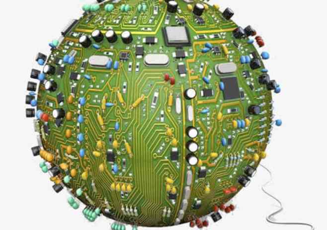
In electronic equipment, printed circuit boardis a key component. It is equipped with other electronic parts and connected to the circuit to provide a stable circuit working environment. So, PCB design and production company circuit board production process are what? Take the six-layer board as an example, let's take a look:
Inner circuit
Copper foil substrate is first cut to size suitable for processing production. Before laminating the substrate, the copper foil on the surface of the substrate should be coarsely treated, and then the dry film should be photoresistant and attached to it at the appropriate temperature and pressure. Then, the substrate is fed into the UV exposure machine for exposure, and the line image on the negative is transferred to the dry film photoresist on the surface of the plate. After the protective film is torn off, the unilluminated area of the film surface is removed with sodium carbonate aqueous solution first, and then the exposed copper foil is corroded with hydrogen peroxide mixed solution to form a circuit. Finally, the dry film was removed by light sodium oxide water solution.
pressing
Before pressing, the inner plate is blackened (oxygenated) to passivate the copper surface to increase the insulation; The copper surface of the inner line is roughened to produce good bonding properties. When overlapping, the inner circuit board above the six layers of the circuit shall be riveted with a rivet machine; Then it is placed neatly between the mirror steel plate with a tray and sent to the vacuum pressing machine to harden and bond the film at appropriate temperature and pressure. The pressed circuit board takes the target hole drilled by the X-ray automatic positioning drilling machine as the reference hole; And the edge of the plate to do appropriate cutting, convenient follow-up processing.
Drilling circuit board factory will circuit board with CNC drilling machine to drill out the interlayer circuit of the gateway and fixed holes of welding parts.
Plated through hole
After forming the interlayer conduction channel, a metal copper layer should be laid on it to complete the interlayer circuit conduction. First, the hair on the hole and the powder in the hole are cleaned by heavy brushing and high pressure washing, and the tin is soaked on the clean hole wall.
Primary copper
The circuit board was immersed in the chemical copper solution, and the copper ion in the solution was deposited on the hole wall to form the through hole circuit; Then the copper layer in the through hole is thickened enough for subsequent processing by copper sulfate bath electroplating.
The secondary copper of the outer line is similar to that of the inner line in the production of the line transfer, but it is divided into positive and negative in the etching of the line. The way of negative film is like the inner line production, after the development of copper directly, to remove the film is completed. The positive method is to add two times of copper and tin lead plating after development. After removing the film, the exposed copper foil is corroded with ammonia water and copper chloride mixed solution to form a line; Finally, the tin - lead layer is removed with the tin - lead stripping solution.
Solderproof ink text printed circuit board factory will be required by the customer's text, trademark or part label in the way of screen printing on the board, and then with hot drying (or ultraviolet irradiation) to harden the text paint ink.

Contact machining
Solderproof green paint covers most of the copper surface of the line, exposing only the terminal contacts for parts welding, electrical testing and circuit board insertion. Appropriate protection layer should be added to the end point to avoid oxides in long-term use, which may affect the circuit stability.
Molding cutting
The circuit board to CNC machine cutting into customer requirements of the appearance of the size; Finally, the dust on the circuit board and the surface of the ion pollutants wash.
Inspection board packing
Commonly used packaging PE film packaging heat shrinkable film packaging vacuum packaging, etc.
PCB design and production company of different types of PCB board PCBA processing
1. Single side patch installation
Add solder paste to component pad. After the solder paste is printed on the bare board of the printed circuit board, the related electronic components are installed by reflow welding, and then reflow welding is performed.
2. Insert unilateral DIP
After the electronic components are inserted by the production line workers, the printed board that needs to be inserted is welded by wave welding. After welding and fixing, it can be cleaned by the method of cutting feet. However, the production efficiency of wave welding is low.
3. Single side mixed loading
PCB board is printed with solder paste, installed with electronic components, and then fixed by reflow welding. After quality check, insert DIP, then wave soldering or hand welding. If there are few through-hole components, manual welding is recommended.
4. Single-side installation and plug-in mix
Some PCB board is double-sided, one side paste, the other side insert. The process of installation and insertion is the same as that of single side machining, but fixture is required for reflow soldering and wave soldering of PCB.
5. Double sided surface mounting
In order to ensure the beauty and function of the PCB, some PCB design engineers will use double-sided mounting. The IC component is arranged on the a side, and the chip component is installed on the b side. Make full use of PCB board space to minimize PCB board surface products.
6. Double-sided mixed loading
There are two ways of double-sided mixing:
In the first way, PCBA assembly is heated three times, which is low efficiency. It is not recommended to use red glue for wave soldering, because the welding qualification rate is low.
The second method is suitable for the situation where there are more patch components on both sides and less THT components, so manual welding is recommended. If there are many THT components, wave soldering is recommended.
PCB basic design process
2023-03-23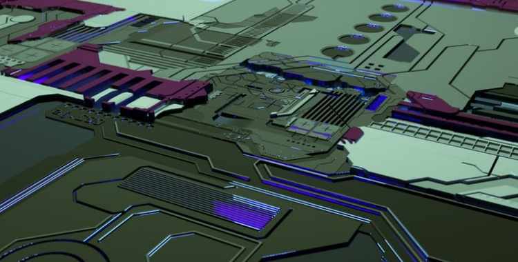


Достаточно загрузить файлы Gerber, BOM и проектные документы, и команда KINGFORD предоставит полное предложение в течение 24 часов.