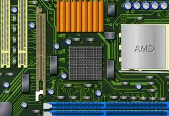
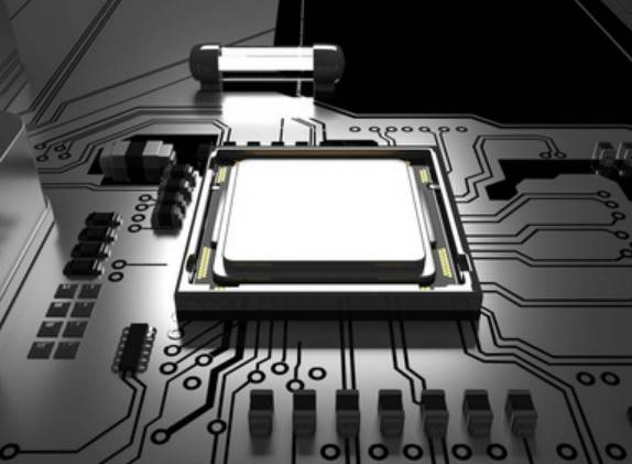
Questions and Answers about experience sharing in high frequency PCB circuit design
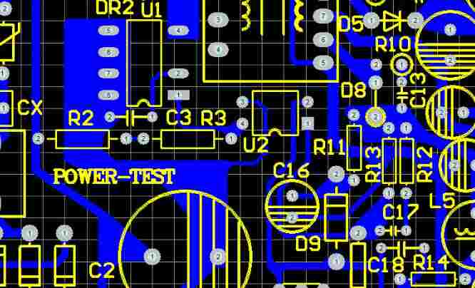
one is that two lines walk on the same layer (side-by-side), the other is that two lines walk on two adjacent layers (over-under). Generally, there are many ways to implement the former side-by-side.