
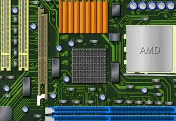
Контрактное производство электроники под ключ в Китае
Шэньчжэнь, район Баоань, улица Фуюн, улица Фуцяо, район 3, промышленный парк Лонгхуй 6


1.2 Delay and timing errors
Signal delay and timing errors are represented by keeping the signal unchanged for some time as it changes between high and low thresholds of the logic level. Excessive signal delay may lead to timing errors and confusion of device functions. Problems often occur when you have more than one receiver. The circuit designer must determine the worst-case time delay to ensure that the design is correct. Cause of signal delay: drive overload, too long cable.
1.3 The logical level threshold has been crossed for several times
The signal may cross the logic level threshold several times during the jump process, resulting in this type of error. Multiple crossing of the logic level threshold error is a special form of signal oscillation, that is, the signal oscillation occurs near the logic level threshold. Multiple crossing of the logic level threshold will result in logic dysfunction. Causes of reflected signals: excessively long lines, unterminated transmission lines, excessive capacitance or inductance, and impedance mismatch.
1.4 Overshoot and undershoot
Overshoot and undershoot are caused by either too long wiring or too fast signal change. Although most components are protected by input protection diodes at the receiver end, sometimes these overshoot levels can go well beyond the component supply voltage range, damaging the component.

1.5 Crosstalk
Crosstalk is represented as when a signal passes on one signal line, the signal adjacent to it will be induced on the PCB board, which is called crosstalk. The closer the signal cables are to the ground wire, the greater the distance between the cables, and the smaller the crosstalk signal generated. Asynchronous signals and clock signals are more prone to crosstalk. Therefore, the way to solve the crosstalk is to remove the crosstalk signal or shield the seriously interfered signal.
1.6 Electromagnetic Radiation
Electro Magnetic Interference (EMI) is a problem caused by excessive electromagnetic radiation and sensitivity to electromagnetic radiation. EMI means that when the digital system is powered on, it will radiate electromagnetic waves to the surrounding environment, thus interfering with the normal operation of the surrounding electronic equipment. The main reason is that the circuit working frequency is too high and the layout is unreasonable. At present, there are software tools for EMI simulation, but EMI emulators are very expensive and the setting of simulation parameters and boundary conditions is difficult, which will directly affect the accuracy and practicability of simulation results. The most common practice is to control the EMI design rules applied in each part of the design, to achieve the rule driving and control in each part of the design.
(2) Methods to avoid transmission line effect
In view of the influence brought by the above transmission line problem, we discuss the following ways to control these effects.
2.1 Strictly control the length of key network cables
If there are high speed jumping edges in the design, the problem of transmission line effect on PCB board must be taken into account. This is especially true of the fast integrated circuit chips with high clock frequencies that are now commonly used. There are some basic principles for solving this problem: If the design is done with CMOS or TTL circuits, the operating frequency is less than 10MHz, and the wiring length should be no more than 7 inches. Operating frequency at 50MHz wiring length should not be greater than 1.5 inches. The wiring length should be 1 inch if the operating frequency is at or above 75MHz. The maximum wiring length for GaAs chips should be 0.3 inches. If you exceed that, you have a transmission line problem.
2.2 Planning the Cable topology properly
Another way to solve the transmission line effect is to choose the correct wiring path and terminal topology. The routing topology refers to the routing sequence and structure of a network cable. When a high-speed logic device is used, the rapidly changing edge signal will be distorted by the branch route of the signal trunk unless the branch length is kept very short. In general, PCB routing adopts two basic topologies, namely Daisy Chain routing and Star distribution.
For Daisy chain wiring, the wiring starts at the driver end and goes to each receiving end in turn. If a series resistor is used to change the signal characteristics, the series resistor should be located next to the driving end. Daisy chain routing has the best effect in controlling the interference of high order harmonics. However, this routing mode has the lowest rate of distribution and is not easy to 100% distribution. In the actual design, we make the branch length of Daisy chain wiring as short as possible, and the safe length value should be: Stub Delay < = Trt *0.1.
For example, the length of the branch end in a high-speed TTL circuit should be less than 1.5 inches. This topology occupies less wiring space and can be terminated by matching a single resistor. However, this routing structure makes the signal receiving in different signal receiving end is not synchronous.


Достаточно загрузить файлы Gerber, BOM и проектные документы, и команда KINGFORD предоставит полное предложение в течение 24 часов.