
Контрактное производство электроники под ключ в Китае
Шэньчжэнь, район Баоань, улица Фуюн, улица Фуцяо, район 3, промышленный парк Лонгхуй 6


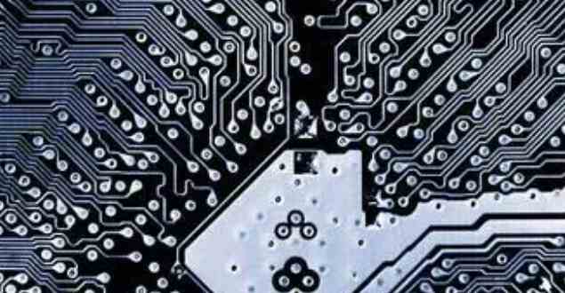
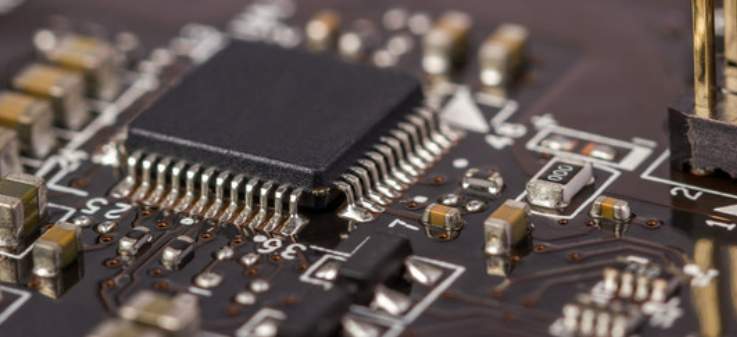
PCB(printed circuit board), the Chinese name is printed circuit board, also known as printed circuit board, is an important electronic component, is the support body of electronic components, is the carrier of electrical connection of electronic components. Because it is produced by electronic printing, it is called "printed" circuit board.
1. How to choose PCB board?
The selection of PCB board must strike a balance between meeting the design requirements and mass production and cost. The design requirements include both electrical and institutional parts. This material issue is often important when designing very high speed PCB boards (frequencies greater than GHz). For example, the now commonly used FR-4 material dielectric loss over a few GHz frequency will have a large effect on signal attenuation and may not be suitable. In the case of electrical dielectric notice whether the dielectric constant and dielectric loss will be dielectric combined at the designed frequency.
2. How to avoid high-frequency interference?
The basic idea of avoiding high-frequency interference is to minimize the interference of high-frequency signal electromagnetic field, which is called Crosstalk. You can increase the distance between the high-speed signal and the analog signal, or add ground guard/shunt traces to the analog signal. Also pay attention to digital ground to analog ground noise interference.
3. How to solve the problem of signal integrity in high-speed design?
Signal integrity is basically a matter of impedance matching. The impedance matching factors include source architecture and output impedance, characteristic impedance of the track, characteristics of the load side, and topology architecture. The way to solve this problem is by termination and adjusting the topology of cable routing.
4. How is the differential wiring mode realized?
Difference pair wiring has two points to pay attention to, one is that the length of the two lines should be as long as possible, the other is that the distance between the two lines (this distance is determined by the difference impedance) to remain unchanged, that is, to keep parallel. There are two parallel modes: one is that two lines walk on the same layer (side-by-side), the other is that two lines walk on two adjacent layers (over-under). Generally, there are many ways to implement the former side-by-side.

5. How to realize differential wiring for clock signal lines with only one output end?To use differential wiring must be the signal source and receiver are also differential signals to make sense. Therefore, it is impossible to use differential wiring for clock signals with only one output.
6. Can a matching resistance be added between the difference line pairs at the receiving end?
The matching resistance between the pairs of difference lines at the receiving end is usually added and its value should be equal to the value of the difference impedance. The signal quality will be better.
7. Why should the wiring of difference pairs be close and parallel?
The wiring of differential pairs should be appropriately close and parallel. differential impedance is an important parameter in the design of difference pairs because the distance affects the value of differential impedance. Parallelism is also required because of the consistency of the differential impedance. If the two lines are far and near, the differential impedance will be inconsistent, which will affect signal integrity and timing delay.
8. How to deal with some theoretical conflicts in actual wiring
Basically, the modular/digital separation is right. Note that the signal should not cross the moat and the returning current path of the power and signal should not be too large.
Crystal oscillator is an analog positive feedback oscillation circuit. To have a stable oscillation signal, it must meet the specifications of loop gain and phase. However, the oscillation specifications of the analog signal are very easy to be interfered, and the interference may not be completely isolated even if ground guard traces are added. And too far away, ground plane noise will also affect the positive feedback oscillation circuit. Therefore, it is necessary to put the distance between the crystal oscillator and the chip as close as possible.
It is true that high speed wiring conflicts with EMI requirements in many ways. However, the basic principle is that some electrical characteristics of the signal cannot fail to meet the specification because of the resistance capacitance or ferrite bead added by EMI. Therefore, it is best to use the technique of arranging wiring and PCB layering to solve or reduce EMI problems, such as high-speed signals going inside the layer. Finally, resistive capacitors or ferrite bead are used to reduce the damage to the signal.
9. How to solve the contradiction between manual wiring and automatic wiring of high-speed signals?
Now the strong wiring software of the automatic wiring most have set constraints to control the winding mode and the number of holes. The winding engine capabilities of each EDA company and the constraint setting projects sometimes differ greatly. For example, whether there are enough constraints to control the way serpentine lines meander or whether the distance between difference pairs can be controlled. This will affect whether the automatic wiring out of the way can conform to the designer's idea. In addition, the difficulty of manually adjusting the wiring also has an absolute relationship with the ability of the winding engine. For example, the pushing capacity of the line, the pushing capacity of the hole, even the pushing capacity of the line against the copper coating, and so on. Therefore, choose a winding engine with strong wiring ability, is the solution.


Достаточно загрузить файлы Gerber, BOM и проектные документы, и команда KINGFORD предоставит полное предложение в течение 24 часов.