
Контрактное производство электроники под ключ в Китае
Шэньчжэнь, район Баоань, улица Фуюн, улица Фуцяо, район 3, промышленный парк Лонгхуй 6

Low cost high density interconnect (HDI) organic substrate is the most important condition for implementing system level packaging (SOP) technology. The crux of the problem is that ultra-precise wires must be etched into an organic plate such as FR4 at very small intervals. The NEMI, SIA, IPC and ITRI research institutes report that substrate suppliers must have the technology to manufacture low-cost fine wires in the future chip design process.
Today, with the increasing trend of integration, many companies are starting to adopt SOC technology. However, SOC cannot solve all system integration problems, so in Packaging Research Centers (PRC) and many other research organizations, System packaging (SOP or SiP) is considered as a supplement to SOC solutions. The integration offered by SOP and SOC can meet the needs of the next generation system design. SOP technologies developed in the PRC include the integration of passive components such as resistors, capacitors, inductors, optical devices, and RF components using the MEMS process, as well as low-cost cooling units, mixed-signal design and testing, related design tools, and low-cost flip chip installation processes that do not use underfill materials.
Of course, SOP technology is based on reliable high density interconnects, processes, and materials, which is the focus of this article. At present, the processing technology of printed wiring board (PWB) lags behind the development of electronic device packaging seriously. The key to solve this problem lies in the lithography technology in the process of routing and perforating. The line width and spacing from 62.5 microns to 25 microns, the processing technology is very different. With the efforts of groups such as ITRI and NEMI, the application of 75 micron to 100 micron wire-width and spacing processes in large area PWBS has become increasingly widespread, resulting in a significant breakthrough in PWB wire-forming technology.
Currently, 30 to 40 micron wire-wide and interwire-wide and 75 to 100 micron micro-perforations can be achieved using the HDI substrate process. PRC is committed to developing processing technologies of 25 microns or less to meet the requirements of precision wiring and line spacing for large area organic panels. The goal is to develop processes for 15 to 25 micron ultra-dense wires and 25 to 50 micron micro-perforations, leading to 6 to 10 micron wires and 10 to 15 micron perforations. MCM Technology Multi-chip module (MCM) technology can meet the requirements of SOP, but the cost is too high.
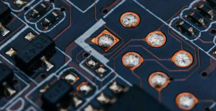
The cabling density of McM-d (deposited MCM) is high and passive components and waveguides can be installed, but production costs are high. McM-c (ceramic MCM) also meets the requirements of SOP and can be integrated into RF structures, however the same cost reasons make it difficult to popularize. Organic multilayer panels are cheap and easy to process, and are suitable for large scale panels, thus meeting the price and performance requirements of the SOP. The PWB manufacturing industry usually refers to a line width of less than 100 microns as "fine line". The current line width can be as small as 50 to 35 microns.

Therefore, the concept of fine line, very fine line and hyperfine line and line spacing is not clearly defined at present. The very fine line discussed in this article refers to the line width of less than 50 microns, which can meet the needs of the industry now and for some time to come. "Uitrafine" refers to a line width of less than 15 microns, which will be required to connect flip chips in fine-spaced arrays in the next few years. PRC is developing low-cost panels to meet the needs of SOP/SLIM for next-generation packaging and other applications. The two key factors affecting "ultra-fine" and "ultra-fine" fine-to-wire processing are:
1, the high resolution photoresistance diagram is printed on the substrate through the design or mask tool;
Summary of practical skills of high frequency PCB design
PCBS are designed to be smaller, faster and less costly. Since the interconnect point is the weakest link in the circuit chain, the electromagnetic property of the interconnect point is the main problem in the engineering design in RF design. It is necessary to investigate each interconnect point and solve the existing problems.
Circuit board system interconnection includes chip to circuit board, PCB board interconnection and signal input/output between PCB and external devices. This paper mainly introduces the PCB board interconnect for high frequency PCB design practical skills summary, I believe that through understanding this paper will bring convenience to the future PCB design.
In PCB design, the interconnection between chip and PCB is important for design. However, the main problem of the interconnection between chip and PCB is that the high interconnection density will lead to the basic structure of PCB material becoming a factor limiting the increase of interconnection density. This article shares practical tips for high frequency PCB design.
For high frequency applications, PCB board interconnect for high frequency PCB design techniques are:
1, the transmission line corner to use 45° Angle, in order to reduce the loss;
2, to use insulation constant value according to the level of strict control of high performance insulation circuit board. This method is beneficial to effectively manage the electromagnetic field between insulation material and adjacent wiring.
3, to improve the PCB design specifications for high-precision etching. Consider again specifying a total error of line width of +/-0.0007 inches, managing undercut and undercut of a wiring shape and specifying siding conditions. The overall management of wiring (wire) geometry and coating surfaces is important to the solution of skin effects related to microwave frequencies and to the implementation of these specifications.
4, the presence of tap inductance, to avoid the use of lead components. At high frequencies, surface mounted components are preferred.
5, for signal hole, to avoid the use of hole processing (pth) process on the sensitive plate. Because this process will cause lead inductance through the hole. Lead inductance can affect layers 4 to 19 if a single through hole in a 20-layer board is used to connect layers 1 to 3.
6, to provide rich ground. Molded holes should be used to connect these connections to prevent the influence of 3 - dimensional electromagnetic fields on the circuit board.
7, to choose non-electrolytic nickel plating or plating process, do not use HASL method for plating. This electroplated surface provides a better skin effect for high frequency current. In addition, this highly weldable coating requires fewer leads, helping to reduce environmental pollution.
8, solder resistance layer can prevent the flow of solder paste. However, due to the uncertainty of thickness and the unknown insulation properties, the entire surface of the plate covered with solder resistance material will lead to a large change in the electromagnetic energy of the microstrip design. Generally, welding dam (solderdam) is used as welding resistance layer.
Why do PCBS now have halogen requirements?
2023-04-12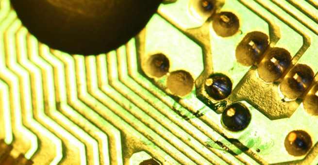


Достаточно загрузить файлы Gerber, BOM и проектные документы, и команда KINGFORD предоставит полное предложение в течение 24 часов.