
Контрактное производство электроники под ключ в Китае
Шэньчжэнь, район Баоань, улица Фуюн, улица Фуцяо, район 3, промышленный парк Лонгхуй 6


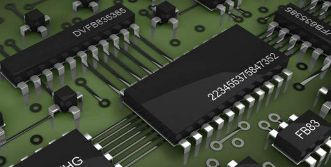
In the process of PCB board wiring design, engineers can be some very important signal lines using ground encircled method, can be in such as clock signals, high-speed analog signals and other signals are not easy to be interfered at the same time in the periphery of the protective ground wire, the signal line will be protected in the middle. Because in the design process, all kinds of signals can not form a loop, the same ground wire can not form a current loop. However, if a loop circuit is generated, it will cause a lot of interference in the system.
The grounding wire surrounding signal wire wiring method can effectively avoid the formation of loop during wiring. One or more high-frequency decoupling capacitors should be located near each integrated circuit block. High frequency choke link should be used when connecting analog ground wire and digital ground wire to public ground wire.
In addition to the several design methods mentioned above, engineers should also try to avoid the branching or stumping of high-speed signal wiring when designing PCB signal wiring. High frequency signal wires walking on the surface tend to generate large electromagnetic radiation, wiring high frequency signal wires between the power supply and ground wire, through the absorption of electromagnetic waves by the power supply and the bottom layer, the radiation generated will be greatly reduced.
Low cost extremely fine copper wire. Of the two factors, the photoresist imaging process is the more critical, and it is difficult to print the target feature geometry onto a low-cost substrate. Compared with the semiconductor process, it can be seen that PWB manufacturing must choose low cost photoresist materials. Another factor to look out for is the substrate. Whereas silicon wafers and other semiconductor substrates have extremely smooth, flat surfaces, low-cost organic sheets such as FR4 have a hard, rough surface, which must be taken into account in the development of new technologies and processes.
Currently, a series of experiments are being conducted to explore the feasibility of machining fine threads on rigid organic sheets. The photoresist materials evaluated included two dry films of different thicknesses and two widely used liquid photoresist materials.

High TgFR4 plates (unclad, single-sided, and double-sided) were used in the process evaluation. In the experiment, the epoxy-based dry film is used to form an electrode - less copper - plated insulating layer between FR4 multilayer plates. The plate in this configuration has a smoother surface than the basic FR4 plate. All photoresist materials are compatible with water soluble processing processes. The length of the test plate is 300 mm. Two liquid photoresists are deposited by rotating coating or meniscus coating. The Dujpont SMVL-100 Vacuum Lamination device layers dry film photoresist C1 (15mm thick) and C2(37.5mm thick) onto the circuit board. In this study, the soft - hard mask method was adopted. Experiments have shown that the use of dry film and liquid photoresist materials can be imaged perfectly on copcopy-covered FR4 plates, with the line spacing of the comb-like structure ranging from 0.635mm (line width/pitch =312 microns) to 0.0508mm(line width/pitch =20/30 microns or line width/pitch =25/25 microns).
A comb structure with a spacing of 50 microns (25 micron wire width and 25 micron wire spacing) can be obtained by addition of copper plating or reduction of etched copper foil. Micrograph of wire width and wire spacing of 15 micron copper wire on dry film photoresist shows that the etched wire is straight, the photoresist adhesion is acceptable, and the edge of the wire is clear. A low cost liquid photoresist material was used to successfully etch 10 micron wire width and line spacing. Using negative liquid photoresist material D, the line width of 7.5 microns can be etched. The experimental results show that with the improvement of machining process and optical mask tools, it will be possible to etch wires finer than 5 microns in the future. In the experimental evaluation of channel interconnection, all materials and processes are compatible with HDI and prior art.
A combination of ultra-fine wire etching, metallization, and microporous interconnect processes enables the fabrication of an array of cop-per stud with a diameter of 35 micron. These arrays form the basis of stacked microporous processes in ultra-HDI substrates. In addition, a series of 35 micron diameter microperforations have been fabricated on the FR4 sheet coated with a thin photosensitive insulating film. After 2,000 thermal cycles, the 50 micron micropore profile demonstrated excellent repeatability with the PRC typical device.
Conclusion The PRC has already implemented 25 micron ultra-fine wire and 15 micron ultra-fine wire HDI technologies, studies below 7.5 micron and line spacing have been completed, and 6 micron wire and line spacing and 10 to 15 micron perforation processes will be developed in the next few years. The next generation of chip technology requires a wire-to-wire spacing of less than 10 microns in order for the SOP technology being developed in the microelectronics industry to be a real success.


Достаточно загрузить файлы Gerber, BOM и проектные документы, и команда KINGFORD предоставит полное предложение в течение 24 часов.