
Контрактное производство электроники под ключ в Китае
Шэньчжэнь, район Баоань, улица Фуюн, улица Фуцяо, район 3, промышленный парк Лонгхуй 6

In the process of PCBA processing, there are often some poor printing problems, which is how to diagnose and deal with it.
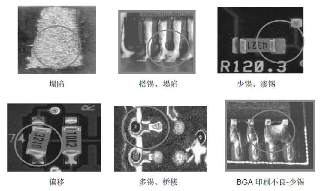
1. Recognition of common poor printing
2. Diagnosis and treatment of tin.
Phenomenon description: There is a little paste between two welding pads. In high temperature welding is often pulled back by the main tin body on the pad, once unable to pull back, will cause short circuit or tin ball, resulting in poor welding.
Diagnosis: small amount of tin powder, low viscosity of tin powder, large particle size of tin powder, high room temperature, printing is too thick, placing pressure, etc.
Tin treatment: increase the proportion of metal composition in tin paste; Increase the viscosity of solder paste; Reduce the size of tin powder; Reduce the temperature (below 270℃); Reduce the thickness of the paste printed (to the overhead height, reduce the pressure and speed of the scraper); Strengthen the precision of the paste; Adjust various construction parameters of solder paste; Reduce the pressure exerted by parts placement; Adjust the temperature curve of preheating and fusion welding.
3. Diagnosis and treatment of tinning.
Phenomenon description: after printing, there is excess solder paste or burr near the solder paste.
Tin penetration diagnosis: insufficient scraper pressure, scraper Angle is too small, steel plate opening is too large, PCB and PAD size is too small, printing is not aligned, printing parameters are not reasonable, PCB and steel plate fitting is not tight, solder paste viscosity is not enough, PCB or steel plate bottom is not clean.
Tinning treatment: adjust the parameters of solder paste printing; Clean or replace template, clean or replace PCB circiut board; Improve the accuracy of printing; Improve the solder paste viscosity.
4. Diagnosis and treatment of tin paste collapse and powder.
Phenomenon description: solder paste on PCB molding is poor, printing height is different, solder paste into powder granular.
Tin paste collapse tin paste powder diagnosis: too much solvent in tin paste, too much solvent at the bottom of the steel plate when wiping, tin paste dissolved in solvent, wiping paper does not rotate, tin paste quality is poor, PCB printing is finished in the air for too long, PCB temperature is too high.
Tin paste collapse powder treatment: improve the proportion of metal in tin paste; Increase the viscosity of solder paste; Reduce the size of tin powder; Reduce the temperature (below 270℃); Reduce the thickness of the paste printed (to the overhead height, reduce the pressure and speed of the scraper); Strengthen the precision of the paste; Adjust various construction parameters of solder paste; Reduce the pressure exerted by parts placement; Avoid placing solder paste and printed circuit board in wet air for a long time; Reduce the activity of flux in solder paste; Reduce the lead content of metals.
5. Diagnosis and treatment of solder paste drawing point.
Description of the phenomenon: The solder paste on the PCB molding is bad, the smear area is too large, the solder joint spacing is too small.
Solder paste drawing point diagnosis: the steel plate opening is not smooth, the steel plate opening size is too small, the demoulding speed is unreasonable, PCB solder joints are polluted, solder paste quality is abnormal, the steel plate is not clean, etc.
Solder paste tip treatment: clean or replace the steel plate; Clean or replace circuit boards; Adjust printing parameters; Replace the better quality solder paste.
6. Diagnosis and treatment of tin deficiency.
Symptom Description: The solder paste on PCB is insufficient.
Diagnosis of less tin: unreasonable orifice size of steel plate, too thin plate mold, plate plug hole, plate pollution, unreasonable demoulding speed and way, etc.
Less tin treatment: increase the thickness of the paste, such as cleaning or replacing the template; Adjust printing parameters; Improve the precision of printing.
7. Diagnosis and management of polytin.
Phenomenon description: The solder paste on PCB welding pad is too much.
Multi tin diagnosis: the steel plate opening size is unreasonable, the plate die is too thick, the room temperature is high, the printing is too thick, the placing pressure is large.
Multi tin treatment: select the appropriate opening form; Reduce the thickness of the paste; Adjust printing parameters; Improve the precision of printing.
8. Diagnosis and treatment of deviation.
Description of the phenomenon: The printed solder paste deviates from the pad on the PCB.
Offset diagnosis: steel plate opening position is unreasonable, PCB positioning is not allowed.
Offset processing: readjust the printing position of PCB board and replace the template to improve the printing accuracy.


Достаточно загрузить файлы Gerber, BOM и проектные документы, и команда KINGFORD предоставит полное предложение в течение 24 часов.