
Контрактное производство электроники под ключ в Китае
Шэньчжэнь, район Баоань, улица Фуюн, улица Фуцяо, район 3, промышленный парк Лонгхуй 6

In order to ensure the PCB substrate for the production of SMT production line, these incoming materials must be tested before production to determine whether they meet the production standards. Inspection of incoming materials is generally carried out by visual inspection in actual production.
The content of PCB incoming material inspection includes PCB size and appearance inspection, PCB warping and distortion detection, PCB weldability test, PCB solder resistance film integrity test, PCB internal defect detection.
1.PCB size and appearance detection
PCB size detection mainly includes: machining hole diameter detection, spacing and tolerance detection and PCB edge size detection.
Appearance detection mainly includes: detection of welding resistance film and pad alignment; Whether the welding resistance film has impurities, peeling, wrinkling and other abnormal conditions; Whether the reference mark is conforming; Circuit conductor width (line width) and spacing meet the requirements; Whether the multilayer board has peeling layer, etc. In practical application, PCB appearance testing equipment is often used to detect it. Typical equipment is mainly composed of computer, automatic workbench, image processing system and so on. This system can detect the inner and outer layers of multilayer board, single/double panel, bottom film; It can detect broken line, connecting line, scratch, pinhole, line width, line distance, rough edge and large area defects.
2.PCB warping and distortion detection
Unreasonable design and improper processing of the process may cause PCB warping and distortion. The test principle is: Expose the PCB under test to a representative thermal environment of the assembly process, and test its thermal stress. Typical thermal stress testing methods are rotary dip tests and solder float tests, in which PCB boards are dipped in molten solder for a certain amount of time and then removed for warping and warping tests.
The PCB warping and warping can be measured manually by placing 3 corners of the PCB against the table top and measuring the distance of the fourth corner from the table top. This method can only be rough estimation, and more effective method is the application of ripple image technology.
3.PCB solderability test
The solderability test of PCB focuses on the test of pad and electroplating through hole. The solderability test method of PCB is stipulated in the IPC-S-804 standard, which includes edge dipping test, rotary dipping test, wave dipping test and solder bead test. Edge dip test is used to test the weldability of surface conductors; Rotary dipping test and crest dipping test are used to test the weldability of surface conductors and electroplating through holes. Solder bead test is only used to test the solderability of electroplating through holes.
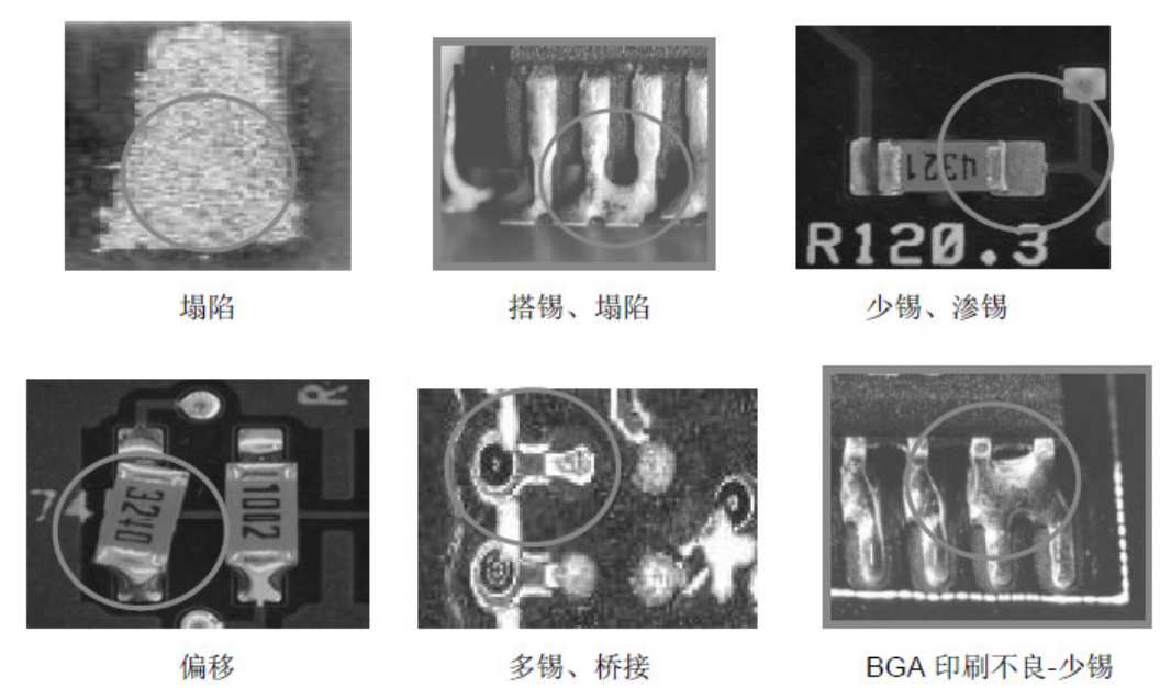
4. Integrity test of PCB solder resistance film
On PCB for SMT, dry film and optical image welding resistance film are generally used, which have high resolution and non-fluidity. Dry film solder resistance film is pressed on the PCB under the action of pressure and heat. It requires a clean PCB surface and an effective laminating process. This kind of solder resistance film has poor viscosity on the surface of tin-lead alloy. Under the impact of thermal stress produced by reflow welding, the phenomenon of stripping and breaking from the surface of PCB often occurs. This kind of welding resistance film is also relatively brittle, and under the influence of heat and mechanical force, micro-cracks may occur. In addition, it is possible to produce physical and chemical damage under the action of cleaning agent. In order to expose the potential defects of dry film solder resistance film, strict thermal stress test should be carried out on PCB during incoming material inspection. This kind of test mostly uses solder floating test, the time is about 10 ~ 15s, solder temperature is about 260 ~ 288℃. When the solder resistance film stripping phenomenon is not observed during the test, the PCB specimen can be immersed in water after the test, and the phenomenon of the solder resistance film stripping can be observed by the capillary action of water between the solder resistance film and the PCB surface. The PCB specimen can also be immersed in SMA cleaning solvent after the test to observe whether it has physical and chemical interaction with the solvent.
5.PCB internal defect detection
The microslice technology is generally used to detect the internal defects of PCB circuit boards. After the solder float thermal stress test, the microslice detection of PCB is carried out. The main detection items include the thickness of copper and tin-lead alloy coating, the interlayer alignment of the conductors inside the multilayer board, lamination voidage and copper cracks.


Достаточно загрузить файлы Gerber, BOM и проектные документы, и команда KINGFORD предоставит полное предложение в течение 24 часов.