
Контрактное производство электроники под ключ в Китае
Шэньчжэнь, район Баоань, улица Фуюн, улица Фуцяо, район 3, промышленный парк Лонгхуй 6

Why do PCB production to do board work?
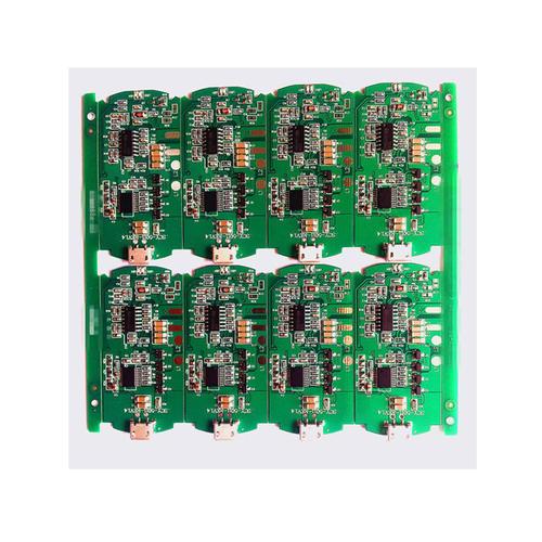
General circuit board production will be carried out board work, its purpose is to increase the production efficiency of SMT production line. PCBS usually have "one in one" boards, such as two in one, four in one... Etc.
If you have a chance to visit the SMT production line, you will find that the biggest bottleneck of the SMT production line is actually in the solder paste printing process, because no matter how big the PCB is, its printing time almost falls around 25 seconds, that is to say, behind the high price of the rapid patch printer, the general use of the patch printer takes less time than the solder paste printer. Will be empty, standing in the economic benefits of the point of view, this is a waste.
In fact, the speed of the SMT machine is very fast, so fast that several parts can be printed in one second, and some of the SMT machines even have several mouthpieces that can be printed at the same time. Judging from the number of parts on the current mobile phone PCBA, if there is only a single board, it should take less than 10 seconds to finish all the SMT operations, so PCB is made into a Mosaic to increase the number of parts. You can increase the utilization rate of the patch machine, improve the efficiency. Of course, it is best to balance the production line so that each unit can be fully functional.
PCB assembling board has another advantage, it can save time when taking and placing PCBA, because multiple boards can be taken and placed at the same time. If the subsequent board level test can be done with board testing, the wasted time of taking and placing boards in the fixture can be greatly saved.
Finally, some boards show irregular shapes when they are designed. If you can design the board, the waste can be greatly reduced. This is the concept of improving the utilization rate of PCB boards.
Disadvantages and limitations of PCB Mosaic board
(1) Although PCB circuit board has many advantages, it still has to be cut into a single board after all PCBA assembly operations are completed. With one more process, it will take more working hours and increase the risk of transporting collision parts.
(2) If there are too small parts such as thin feet and 0201 on some boards, the number of plates cannot be too much, because there are tolerances between boards and boards. If there are too many plates, it may cause the tolerance to be too large to meet the accuracy requirements of solder paste printing, and finally, solder paste printing bias and solder problems.

(3) It is not recommended that the number of PCB is too much for some too thin PCB, because the thinner the PCB is, the greater the deformation, the number of plate is too varied and wide, and the patch and welding furnace are a test. Of course, this aspect can be overcome by using the furnace vehicle or the whole vehicle, but the cost of the vehicle and increased labor costs have to be considered.
What is the purpose of PCB making edge?
The PCB board edge is also called coupon in foreign countries. Because it is similar to discount coupons from super retailers, you can break off the excess board edge directly. However, for quality consideration, we do not recommend that you break off the excess board edge by hand.
PCB board edge design is mainly used to assist assembly and production. In fact, the SMT production line is highly automated at present, and the delivery of boards depends on belts and chains. As a smart person, you should have thought that the main purpose of the board edge is to transport boards for these belts and chains.
Of course, if you want, you can also leave some space around the board do not put any electronic parts, generally required to keep at least 5.0mm above, because the chain of the welding furnace needs to use a relatively deep plate edge position, so you have the opportunity to not need to design the edge, otherwise the belt and chain may damage the electronic parts around it.
In addition, PCB board edge has other uses:
(1) Fixture holes can be placed for positioning the board during ICT or FVT testing after SMT process, so as to prevent the needle bed from being out of position with the test point.
(2) As SMT production line sensor to detect the position of the circuit board. Generally, each machine on the SMT production line will have a sensor to detect the arrival of subsequent boards, so as to ensure that only one piece of board is working in the machine. Otherwise, another piece of board will bump into the machine before the SMT operation of the previous piece of board is completed, and the machine will be in chaos, and it will be hard to know which piece of board to hit. The appearance of some boards may be just in the place where sensors of the SMT production line are detected, usually at the leading edge of the upper left corner of the circuit board. In this case, the edge of the board can be used to achieve the purpose of solid sensor detection.
(3) When too many positioning optical points cannot be set in some boards due to space limitations, they can also be placed at the position of the edge of the board, but it is suggested that the parts disk near the thin interfoot inside the board should also have positioning points, which can increase the accuracy of the patch.
Why should the PCB board plug the hole?
2023-02-18


Достаточно загрузить файлы Gerber, BOM и проектные документы, и команда KINGFORD предоставит полное предложение в течение 24 часов.