
Контрактное производство электроники под ключ в Китае
Шэньчжэнь, район Баоань, улица Фуюн, улица Фуцяо, район 3, промышленный парк Лонгхуй 6

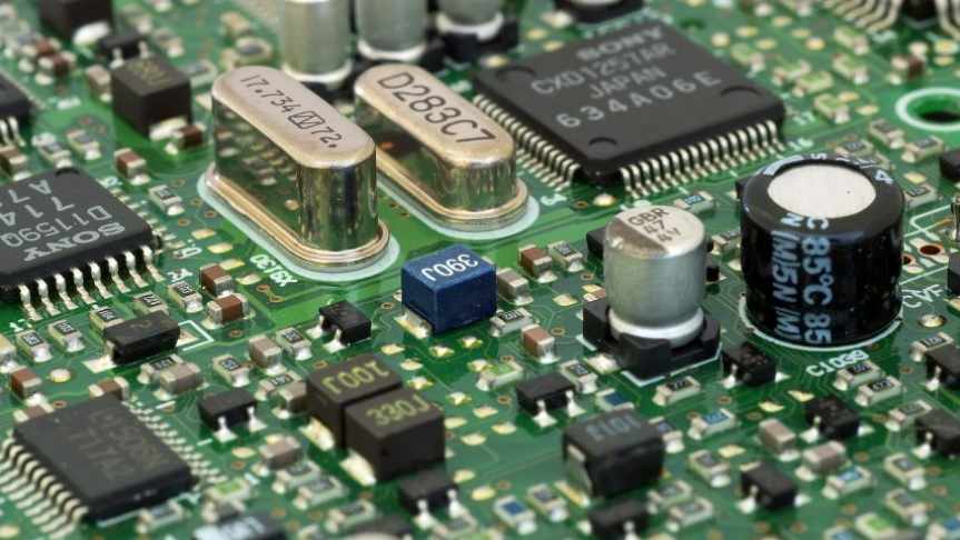
The purpose of testing PCB board is to find out the defects of PCB board and repair them to ensure the production quality of PCB board and improve the qualified rate of products. At present, PCB board testing methods can be divided into two categories: electrical testing methods and visual testing methods. Today Xiaobian and you share 7 commonly used PCB detection methods, as follows:
1. Manual eye test
Manual visual inspection of PCBS is the most traditional inspection method, with the advantages of low initial cost and no test fixture. Use a magnifying glass or calibrated microscope to visually inspect the PCB board and determine when corrective action is required. The disadvantages of manual visual test are subjective human error, high long-term cost, discontinuous defect detection and difficult data collection. With the increase of PCB production and the reduction of wire spacing and component volume on PCB, the manual eye test method is becoming less and less feasible.
2. Size check
The hole position, length and width, position, and other dimensions are measured using a two-dimensional image measuring instrument.Since PCBS are thin and soft products, contact measurements can easily be deformed, resulting in inaccurate measurements.Two-dimensional image measuring instrument has become the best high precision dimension measuring instrument.Image measuring instrument can realize automatic measurement after programming, not only the measurement accuracy is high, but also greatly shorten the measurement time, improve the measurement efficiency.3. Test online
There are several testing methods, such as the needle bed tester and the flying needle tester. Identify manufacturing defects through electrical performance testing and test analog digital and mixed-signal components to ensure they meet specifications. The main benefits are low testing cost per board, powerful digital and functional testing capabilities, fast and thorough short and open circuit testing, programming firmware, high defect coverage, and ease of programming. The main disadvantages are the need to test the fixture, programming and debugging time, the high manufacturing cost of the fixture, and the difficulty to use.
4. Functional system test
Functional testing is the earliest principle of automatic testing. It is a comprehensive test of the functional modules of the circuit board at the middle stage and end of the production line using special testing equipment to confirm the quality of the circuit board. Functional system testing is based on specific boards or specific units, and can be done using a variety of devices. There are final product tests, up-to-date physical models, and stack tests. Functional testing usually does not provide in-depth data to improve the process, but rather requires special equipment and specially designed testing procedures. Because writing functional test programs is very complex, it is not suitable for most circuit board production lines.
5. Laser detection system
Laser detection involves scanning the printed board with a laser beam, collecting all the measured data, and comparing the actual measured value with the preset qualified limit value. This is the latest development in PCB testing technology, which has been proven on bare boards and is being considered for assembly board testing. The main advantages are fast output, no fixed fixtures and barrier-free visual access; Disadvantages are high initial cost, maintenance and usage problems.
6. Automated X-ray screening
Automated X-ray inspection is used to detect defects in ultra-fine-spaced and ultra-dense circuit boards, Bridges, missing chips, poor alignment, and other defects that occur during assembly. The principle of testing is to use differences in X-ray absorption rates of different substances to examine the part to be tested and look for defects. It can also be used to detect internal defects in IC chips, which is the only way to test the welding quality of the ball grid array and solder ball. The main advantage is the ability to detect BGA welding quality and embedded components without the cost of fixtures.
7. Automatic optical inspection
Automatic optical inspection, also known as automatic appearance inspection, is a relatively new method for identifying manufacturing defects. It is based on optical principles and makes full use of image analysis, computer and automatic control techniques to detect and treat defects encountered in production. AOI is commonly used before and after reflow and before electrical testing to improve compliance rates for electrical handling or functional tests. At this point, the cost of correcting the defect is much lower than the cost after the final test, generally more than ten times.
The above are seven commonly used PCB detection methods. Although there are a variety of PCB detection methods, optical inspection and X-ray inspection are the most popular ones on the market.


Достаточно загрузить файлы Gerber, BOM и проектные документы, и команда KINGFORD предоставит полное предложение в течение 24 часов.