
Контрактное производство электроники под ключ в Китае
Шэньчжэнь, район Баоань, улица Фуюн, улица Фуцяо, район 3, промышленный парк Лонгхуй 6

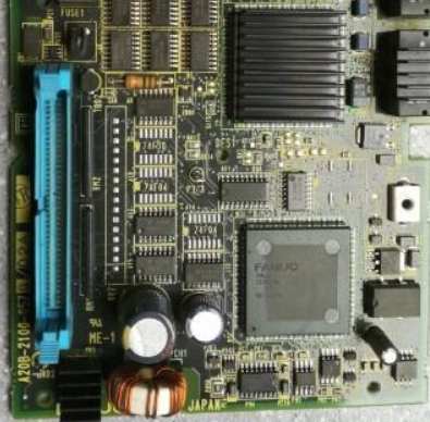
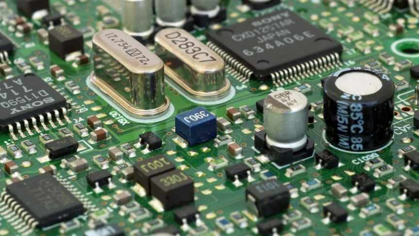
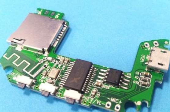
In PCBA patch processing, no matter reflow welding or wave soldering, some holes (bubbles) will inevitably appear after cooling PCBA solder joints. The main reason for the void in the solder joint is that the bubbles produced by the pyrolysis of organic matter in the flux cannot escape in time. The flux has been consumed in the reflux area, and the viscosity of the solder paste has changed greatly. At this time, the flux in the solder cracks, resulting in the bubble after high temperature cracking did not overflow in time, and was encapsulated in the solder joint, forming a cavity phenomenon after cooling. Next, PCBA patch processing factory -kingford for you to elaborate analysis, hope to bring you some help!
1. Influence of flux activity
Due to the high temperature pyrolysis of the organic matter in the flux, it is difficult for the air bubbles to escape, resulting in the gas being wrapped in the alloy powder. From the process can be seen, organic matter by the heat produced by the main way of bubbles are: solder paste in the flux, other organic matter, wave soldering flux or impurities. These organic compounds decompose at high temperatures to form gases. Due to the relatively small proportion of gas, the gas will be suspended on the surface of the solder during welding, and the gas will eventually escape and not stay on the surface of the alloy powder. However, the surface tension of the solder and the gravity of the part to be welded must be considered when welding. Therefore, the surface tension of the solder paste and the gravity of the component should be combined to analyze why the gas cannot escape from the surface of the alloy powder, thus forming the cavity. If the buoyancy of the gas produced by organic matter is less than the surface tension of the solder, then the organic matter in the flux after pyrolysis at high temperature, the gas will be surrounded in the interior of the welding ball, the gas will be deeply absorbed by the welding ball, at this time it is difficult for the gas to escape, and then form a cavity phenomenon.
2. It is related to the oxidation degree of PCB pad
The higher the degree of oxidation and dirt on PCB pad surface, the more holes will be generated by PCBA solder joints after welding. Because the greater the degree of oxidation of the pad, the stronger the active agent is needed to treat the oxide on the surface of the welded object. Especially for the OSP(organic solvent preservative) surface treatment, an organic protective film on the OSP pad is difficult to remove. If the oxide on the surface of the pad is not removed in time, the oxide will remain on the surface of the object to be welded. At this time, the oxide will prevent the alloy powder from contacting with the surface of the metal to be welded, resulting in the formation of a bad welding rejection phenomenon. The surface oxidation is serious, and the organic gas decomposed at high temperature will hide in the alloy powder. At the same time, the lead-free surface tension is large, the alloy proportion is relatively large, the gas is difficult to escape, the gas will be surrounded in the alloy powder. Oxide on the surface of the solder paste and the metal to be welded must be avoided. Otherwise, there is no other way to reduce cavity formation.
3, the effect of solvent boiling point
Whether it is the solvent before wave soldering or solder paste itself, the boiling point between the two directly affects the size of PCBA solder joint cavity and the probability of cavity formation. The lower the boiling point of the solvent, the more likely it is to form voids. So you can choose a solvent with a high boiling point to avoid cavitation. If the boiling point of the solvent is low, the solvent will evaporate in the constant temperature zone or reflux zone, leaving only the high viscosity and difficult to move organic matter, which must be surrounded. Therefore, when choosing solder paste, try to choose solder paste with high boiling point solvent to reduce the occurrence of cavitation phenomenon.

4, and welding time
The impregnation time of Sn63-Pb37 solder is very short, about 0.6 s versus 1.5 s of SnAgCu solder, while the surface tension of lead-free solder is high, the movement speed is slow, and the solder is less wettability and diffusivity than that of lead solder. In these cases, the gas produced by the pyrolysis of organic matter is difficult to escape, and the gas will be completely surrounded in the alloy layer. Of course, the probability of bubbles in lead-free solder is much greater than that in lead, which is also the problem and challenge faced by the lead-free welding process in PCBA patch processing today.
5. Caused by excessive absorption of moisture in the air by tin paste
Solder paste should be used according to the correct method. After the solder paste is removed from the refrigerator, it should be kept at room temperature (25 ° C ±3 ° C) for at least 4 hours. When the solder paste is preheating, remember that the lid of the solder paste cannot be opened in advance, and the solder paste cannot be preheated. Also, avoid inhaling moisture in the air. Solder paste must be stirred before online use. The purpose is to mix the alloy powder and flux evenly. In the mixing process, the time should not be too long (about 3-5min), mixing force should not be too large. If the force is too strong for too long, the alloy powder may be crushed, causing the metal powder in the solder paste to oxidize. If the solder paste powder is oxidized, the probability of holes will be greatly increased after flow welding. After printing, the solder paste cannot be placed in the air for too long (generally within 2 hours), otherwise the solder paste absorbs too much water, which will increase the probability of the formation of the cavity. It can be seen that the correct use of welding paste is very important and must be carried out in accordance with the correct use of welding paste, otherwise the welding defects after reflow welding of PCBA will be greatly increased. Therefore, the correct use of welding paste will be a prerequisite to ensure the quality of various welding, must be attached great importance to.
With the rapid development of PCBA patch processing industry, the component density is getting higher and higher, and the number of PCB substrate layers is increasing, which poses new challenges to the PCBA patch processing technology. For the reliability of PCBA, once the void area of solder joint exceeds the IPC standard, it will not only affect the mechanical properties of components, but also affect the electrical properties of the whole product. The void phenomenon will bring incalculable risk to the solder joint. Therefore, PCBA plus factory strict control of PCBA solder joint cavity (bubble) is very important, must pay great attention to.


Достаточно загрузить файлы Gerber, BOM и проектные документы, и команда KINGFORD предоставит полное предложение в течение 24 часов.