
Контрактное производство электроники под ключ в Китае
Шэньчжэнь, район Баоань, улица Фуюн, улица Фуцяо, район 3, промышленный парк Лонгхуй 6

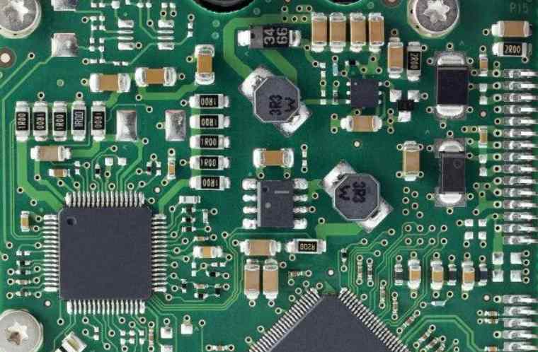
PCB production is generally divided into: PCB layout → core board production → inner PCB layout transfer → core board drilling and inspection → lamination → drilling → copper chemical precipitation in hole wall → outer PCB layout transfer → computer control and copper plating. The specific operation process is as follows:
1.PCB Layout
When a PCB manufacturer receives a CAD file from a customer, because each CAD software program has its own unique file format, the PCB manufacturer usually translates the CAD file from the customer into a unified format -- Extended Gerber RS-274X or Gerber X2. After that, the engineer will check whether the PCB layout conforms to the production process and whether there are defects.
2. Manufacture of core board
Clean the copper coated plate to prevent the circuit from short circuit or break due to dust. The 8-layer PCB is actually made up of 3 copper-coated plates (core plate) plus 2 copper films and then bonded together with semi-cured sheets. The production sequence starts with the core board in the middle (four or five layers of wiring), which is constantly stacked on top of each other and then fixed. The production of 4-layer PCB is similar, but only uses 1 core board and 2 copper films.
3. Transfer of inner PCB layout
First, the two layers of the Core board are made. After cleaning, the copper-coated sheet is covered with a sensitive film. The film solidifies when exposed to light, forming a protective film over the copper-coated copper foil. The two layers of PCB layout film and the double layer of copper-coated plate are inserted into the top layer of PCB layout film at last to ensure the precise layering position of the two layers of PCB layout film
Sensitizer uses UV lamp to irradiate the sensitive film on the copper foil. Under the transparent film, the sensitive film is cured. Under the opaque film, there is no curing sensitive film. The copper foil covered under the cured photosensitive film is the required PCB layout circuit, and then the uncured photosensitive film is cleaned with lye. The required copper foil circuit will be covered by the cured photosensitive film. The unwanted copper foil is then etched away with a strong base, such as NaOH. Tear off the cured photosensitive film to expose the required PCB layout line copper foil.
4. Drill holes and check the core plate
After the core board is successfully made, make a matching hole on the core board to facilitate alignment with other raw materials.
Once the core board is pressed together with other layers of PCB, it cannot be modified, so the inspection is very important. The machine will automatically compare with the PCB layout drawing to check the error. In this way, the first two layers of PCB board have been made.
5. Laminate
There is a need for a new material called semi-cured sheet, which is core board and core board (PCB layers>4), and the adhesive between the core plate and the outer copper foil, but also play the role of insulation. The lower copper foil and two layers of semi-cured sheet have been fixed through the alignment hole and the lower iron plate in advance, and then the made core plate is also placed into the alignment hole, and finally the two layers of semi-cured sheet, a layer of copper foil and a layer of pressured aluminum plate are covered on the core plate in turn.
The PCB board sandwiched by the iron plate is placed on the bracket, and then sent to the vacuum hot press for laminating. The heat of a vacuum hot press melts the epoxy resin in the semi-cured sheet, holding the core plates and the copper foil together under pressure. After laminating, remove the top iron plate pressing the PCB. The pressurized aluminum plate is then removed. The aluminum plate also acts as a barrier between the different PCBS and keeps the copper foil on the PCB smooth. Both sides of the PCB will be covered by a layer of smooth copper foil.
6. Drill a hole
First, perforations are drilled through the PCB, and then the hole walls are metallized to conduct electricity. Place a sheet of aluminum on the punch machine tool and place the PCB on top of it. To improve efficiency, one to three identical PCB boards are stacked on top of each other, depending on the number of PCB layers. Finally, the top PCB is covered with a layer of aluminum. The upper and lower layers of aluminum are so that when the bit is drilled in and out, the copper foil on the PCB will not be torn.
The operator then only needs to select the correct drilling procedure, the rest is done automatically by the drilling machine. The drill bit is driven by air pressure and can rotate at up to 150,000 revolutions per minute, which is high enough to keep the wall smooth. Drill bit replacement is also done automatically by the machine according to the program. The smallest drill bit can be 100 microns in diameter, while the diameter of a human hair is 150 microns. It was removed because the melted epoxy had been squeezed to the outside of the PCB circuit board during the previous laminating process. A die milling machine cuts the PCB periphery according to the correct XY coordinates.
7. Copper chemical precipitation of pore wall
The first step is to accumulate a layer of conductive material on the pore wall, and form a 1 micron copper film on the entire PCB surface, including the pore wall, by chemical deposition. The whole process such as chemical treatment and cleaning is controlled by machines.
8. Transfer of outer PCB layout
The outer PCB layout transfer adopts the normal method, using positive plate as the board. The PCB layout of the outer layer is transferred to the copper foil, using photocopied film and sensitive film to transfer the PCB layout to the copper foil. The PCB is covered by the cured photosensitive film for the non-line area. The uncured photosensitive film is cleaned and then electroplated. Where there is a film can not be electroplated, and where there is no film, first plated with copper and then plated with tin. After the film is removed, alkaline etching is carried out and finally tin is removed. The line pattern is left on the board because it is protected by tin.
Clean both sides of the copper foil PCB into the film pressing machine, the film pressing machine will be sensitive to the copper foil molding. The upper and lower layers of photocopied PCB layout film are fixed through the positioning hole, and the PCB board is placed in the middle. The photosensitive film under the permeable film is then cured by UV light, which is the line that needs to be preserved. After cleaning away any unwanted, uncured photosensitive film, inspect it. Clamp the PCB and electroplate the copper onto it. To make sure the holes are conductive enough, the copper coating on the holes must be 25 microns thick, so the system will be controlled by a computer to ensure accuracy.
9. Computer control and copper plating
After the copper film is plated, the computer also arranges for a thin layer of tin to be plated. Check after unloading the tinned PCB board to ensure the correct thickness of plating copper and tin. The etching process is then completed by a complete automated pipeline. First of all, the photosensitive film on the PCB board is cured. It is then washed with a strong alkali to remove the unwanted copper foil covered by it. Then remove the tin coating on PCB layout copper foil with the tin solution. Finally, after cleaning, the 4-layer PCB layout is completed.
7 commonly used PCB board detection methods
2023-03-16


Достаточно загрузить файлы Gerber, BOM и проектные документы, и команда KINGFORD предоставит полное предложение в течение 24 часов.