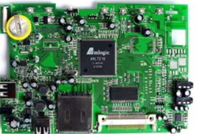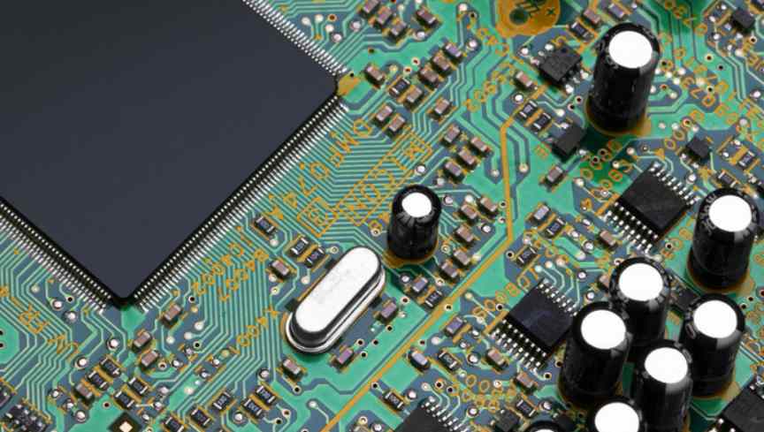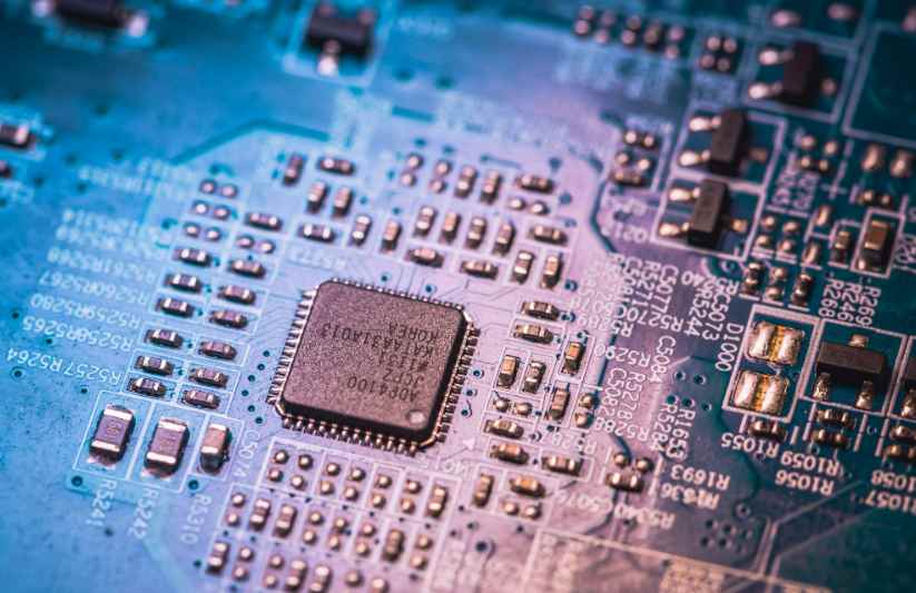
EMC problem is very important in PCB design, which plays a decisive role in PCB quality and performance stability. Next, kingford, Shenzhen PCB design company, would like to share with you the factors related to EMC problems in PCB design?
Factors related to EMC issues in PCB design
1. System Design:
In the design of system-level EMC, EMI interference sources should be determined first, so as to gradually better shield EMI radiation sources.
2. Influence of structure:
If the radiation harassment emission of non-metallic chassis exceeds the standard, measures such as conductive spraying, partial shielding design, cable shielding, and proper grounding should be taken.
3. Cable influence:
Do not use cable shielding as a signal return channel.
4. Component selection is related:
Take varistor as an example: varistor is mainly characterized by a wide range of working voltage, voltage protection, lightning protection, suppression of surge current, absorption of peak pulse, amplitude limiting, noise elimination and other functions.
5. Related to SI/PI simulation:
Before and after the EMC design of boards is complete, you need to compare and verify the overall EMC simulation of boards, and even the improvement effects of some major EMC design measures.
Step 6 Ground
Grounding Purpose: To establish a low-impedance path between the device shell and nearby metal conductors. When there is leakage current in the device, personal safety is not endangered.
7. The relationship between PCB design.
When the RF current in the PCB board passes through, when the current passes through the closed circuit, the magnetic field will be generated; At the same time, it also generates a radiating electric field. This is the main cause of radiation interference caused by PCB board of switching power supply.
8. Software anti-interference technology:
Including redundancy technology, fault tolerance technology, marking technology, digital filtering technology.
9. Blocking:
Electromagnetic shielding is an effective method to suppress interference in the form of field.
10. Filtering:
Filtering technology is the main means to suppress the electromagnetic interference conducted by electrical and electronic equipment, improve the anti-interference level of electrical and electronic equipment, and also an important auxiliary measure to ensure the overall or local shielding efficiency of equipment.
2. Cause analysis of PCB board surface bubbling
Board bubbling is one of the common quality defects in PCB production. Because of the complexity of PCB production process, it is difficult to prevent the surface foaming defects.
PCB board surface bubbling cause
1. Substrate processing problems. For some thinner substrate, due to the poor rigidity of the substrate, it is not suitable to brush the board. Therefore, in the process of production and processing, attention should be paid to control, so as not to cause the poor adhesion of copper foil and chemical copper substrate surface bubbling.

2, board processing (drilling, laminating, milling, etc.) caused by oil, or other liquid caused by dust pollution, will lead to bubbling board.
3. Bad copper brush plate. The pressure of grinding plate is too high before copper sinking, resulting in orifice deformation, orifice bubbling in the process of copper sinking, electroplating, tin spraying and welding.
4. Wash in water. Because copper plating needs a large number of chemical solution treatment, and acid, alkali, inorganic, organic and other medical solvents, not only will cause cross pollution, but also cause local poor treatment of the board, leading to some adhesion problems.
5. Microetching in pre-treatment of copper plating and pattern plating. Excessive microetching can cause substrate leakage at the orifice and blistering around the orifice.
6. The activity of copper precipitated liquid is too strong. The high content of three components in the newly opened copper cylinder or bath leads to the degradation of the physical properties and poor adhesion of the coating.
7. Oxidation of the plate surface in the production process will also lead to bubbling of the plate surface.
8. Poor rework of copper mine. In the repair process of some copper plated repair plates, due to poor deplating, incorrect repair method or improper control of micro-corrosion time in the repair process, the surface of the plate will appear foaming phenomenon.
9. Insufficient washing after development, storage time after development is too long or too much dust in the workshop during text transfer will cause potential quality problems.
10. Before copper plating, the pickling tank should be replaced in time, otherwise it will not only cause the cleanliness of the board, but also cause the surface roughness and other defects.
11, organic pollution, especially oil pollution, will make the plate surface in the plating tank foaming.
12, in the production process to pay special attention to the plate charging, especially with air stirring bath.
The above is the reason analysis of PCB surface foaming. Hope to help the industry peers! In the actual production process, there are many reasons why the surface of the board bubbles. Look at it on a case-by-case basis, don't generalize.
kingford PCB design capability
Maximum signal design rate: 10Gbps CML differential signal;
Maximum number of PCB design layers: 40;
Minimum line width: 2.4mil;
Minimum line spacing: 2.4mil;
Minimum BGA PIN spacing: 0.4mm;
Minimum mechanical hole diameter: 6mil;
Minimum laser drilling diameter: 4mil;
Maximum number of pins:; 63000 +
Maximum number of components: 3600;
Maximum number of BGA: 48+.


