
Контрактное производство электроники под ключ в Китае
Шэньчжэнь, район Баоань, улица Фуюн, улица Фуцяо, район 3, промышленный парк Лонгхуй 6

With the development of electric age, there are more and more electromagnetic wave sources in human living environment, such as radio broadcasting, television and microwave communication. Electrical appliances for household use; Power frequency electromagnetic field of transmission line; High frequency electromagnetic field, etc. When the field intensity of these electromagnetic fields exceeds a certain limit and the operation time is long enough, it may endanger human health. It can also interfere with other electronic devices and communications. All of these need to be protected. The concepts of electromagnetic interference and shielding are often put forward in the development, production and use of electronic products. The core of electronic products in normal operation is a coordination process between the circuit board and the components and components installed on it. It is very important to improve the performance of electronic products and reduce the influence of electromagnetic interference.
1.PCB board design
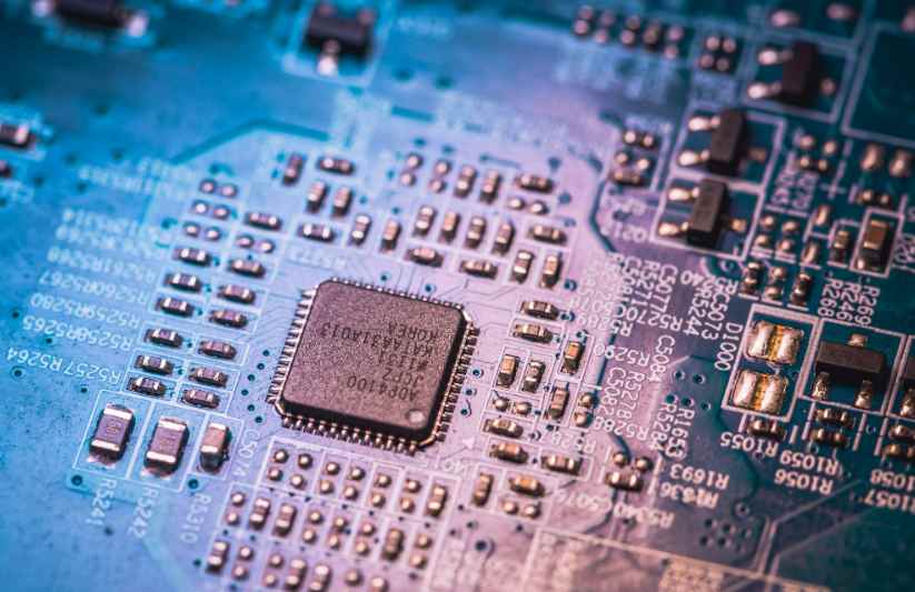
Printed circuit board (PCB) is the electrical connection between circuit components and devices in electronic products. It is the most basic component of various electronic equipment. The performance of PCB is directly related to the quality and performance of electronic equipment. With the development of integrated circuit, SMT technology and micro-assembly technology, there are more and more electronic products with high density and multiple functions. As a result, the PCB wire layout is complex, zero parts, many components and dense installation, which will inevitably make the interference between them more and more serious. Therefore, the problem of suppressing electromagnetic interference has become the key to the normal operation of an electronic system. Similarly, with the development of electrical technology, PCB density is getting higher and higher, PCB design quality has a great impact on the circuit interference and anti-interference ability. In addition to the selection of components and circuit design, good PCB design is also a very important factor in electromagnetic compatibility in order to obtain the best performance of electronic circuits.
(1) Reasonable PCB layer design
According to the complexity of the circuit, the reasonable selection of PCB layer mathematics can effectively reduce the electromagnetic interference, greatly reduce the volume of PCB and the length of current loop and branch line, and greatly reduce the cross interference between signals. The experiment shows that the noise of four-layer plate is 20dB lower than that of double-layer plate when the same material is used. However, the higher the number of plates, the more complex the manufacturing process and the higher the manufacturing cost. In the multilayer wiring, it is best to adopt the "well" pattern network wiring structure between the adjacent layers, that is, the direction of the adjacent layers are perpendicular to each other. A printed board, for example, is wired horizontally on the top side, lengthwise on the bottom side, and connected through holes.
(2) Reasonable PCB size design
When the size of PCB board is too large, it will lead to the growth of printed wire, increase impedance, decrease anti-noise ability, and increase the cost of equipment volume. If the size is too small, the heat dissipation is not good, and the adjacent lines are susceptible to dry disturbance. In general, the Mechanical Layer is used to determine the physical border, that is, the outline size of the PCB, and the Keepout Layer is forbidden to determine the layout and effective area of the wiring. In general, according to the number of functional units of the circuit, all components of the circuit are overall, and finally determine the best shape and size of the PCB board. Usually a rectangle is chosen, with a aspect ratio of 3:2. When the size of the circuit board is larger than 150 mmx200 mm, the mechanical strength of the circuit board should be considered.
2. PCB layout
In PCB design, product designers often only focus on improving density, reducing space occupation, simple production, or the pursuit of beauty, uniform layout, ignoring the influence of circuit layout on electromagnetic compatibility, so that a large number of signals radiate into the space and form mutual interference. A poor PCB wiring can cause more EMC problems than it can eliminate them.
In electronic equipment, digital circuit, analog circuit and power circuit components layout and wiring characteristics are different, they produce interference and interference suppression methods are different. Because the frequency of high frequency and low frequency circuit is different, its interference and the method of suppressing interference are different. Therefore, in the component layout, the digital circuit, analog circuit and power circuit should be placed separately, the high-frequency circuit and the low-frequency circuit separated. Conditions should be made each self-isolation or separate into a circuit board. In the layout, special attention should be paid to the distribution of strong and weak signals and signal transmission direction.
The layout of PCB components and other logic circuits, should be put as close to each other as possible, so that better anti-noise effect can be obtained. The placement of components on the printed circuit board should be subject to electromagnetic interference. One principle is to keep the leads between the components as short as possible. In the layout, the analog signal part, high-speed digital circuit part, noise source part (such as relay, large current switch, etc.) should be separated reasonably, so that the signal coupling between each other is minimal.
Clock generator, crystal oscillator and CPU clock input are easy to produce noise, should be closer to each other. Devices, small current circuits and large current circuits that are easy to generate noise should be kept away from logic circuits as far as possible. If possible, it is important to make a separate circuit board.
General layout requirements for PCB components: Circuit components and signal paths must be laid out to minimize coupling of unwanted signals.
(1) Low level signal channels should not be near high level signal channels and unfiltered power lines, including circuits that can generate transient processes.
(2) Separate the low level analog circuit from the digital circuit to avoid the common impedance coupling between the analog circuit, the digital circuit and the common circuit of the power supply.
(3) High, medium and low speed logic circuits should be used in different areas on the PCB.
(4) The circuit should be arranged so that the length of the signal line is minimum.
(5) Ensure that there are no long parallel signal lines between adjacent boards, between adjacent layers of the same board and between adjacent wiring on the same level.
(6) Electromagnetic interference (EMI) filter should be as close to the source of electromagnetic interference as possible, and placed on the same circuit board.
(7)DC/DC converters, switching components and rectifiers should be placed as close as possible to the transformer to minimize its wire length.
(8) Place the voltage regulator and filter capacitor as close to the rectifier diode as possible.
(9) Printed boards are partitioned according to frequency and current switching characteristics, and the distance between noisy and non-noisy components should be further away.
(10) The wiring sensitive to noise should not be parallel to the high-current and high-speed switching lines.
(11) component layout should pay special attention to the problem of heat dissipation, for high-power circuits, should be those heating components such as power tube, transformer and so on as far as possible to the side of the distributed layout, easy to heat distribution, do not concentrate in one place, do not high capacitance too close to avoid premature aging of electrolyte.
PCB wiring
A PCB is constructed using a series of laminated, routed and prepreg layers on a vertical stack. In multilayer PCBS, the signal wire is placed on the outermost layer for easy debugging.
At high frequency, distributed inductance and capacitance of wiring, through-hole, resistor, capacitor, and connector on the printed circuit board cannot be ignored. Resistance produces reflection and absorption of high frequency signals. The distributed capacitance of the line also comes into play. When the length of the line is greater than 1/20 of the wavelength corresponding to the noise frequency, the antenna effect occurs and the noise is emitted outward through the line.
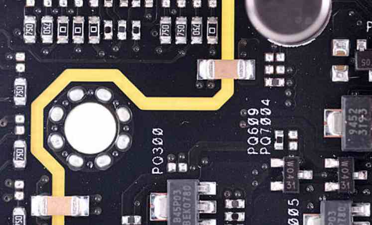
Wiring of printed circuit boards is mostly done through holes. One pass hole can bring about 0.5 pF of distributed capacitance, and reducing the number of pass holes can significantly increase the speed.
An integrated circuit itself is encapsulated in a material that introduces 2 ~ 6 pF capacitors. A connector on the circuit board with 520 nH distributed inductance. A dual in-line 24-pin integrated circuit socket with 4 ~ 18 nH distributed inductors.
General requirements to avoid the influence of PCB routing distribution parameters:
(1) Increase the distance between the wires to reduce the crosstalk of capacitive coupling.
(2) Double panel wiring, the two sides of the wire should be perpendicular to each other, oblique, or curved line, avoid parallel to each other, to reduce parasitic coupling; As the input and output of the circuit with the printed wire should be as far as possible to avoid rabbit adjacent parallel, so as to avoid the occurrence of backpropagation, in these wires had better add ground wire.
(3) The sensitive high-frequency wire is placed far away from the high-noise power line to reduce the coupling between each other; The high frequency digital circuit is thinner and shorter.
(4) Widen the power cord and ground wire to reduce the impedance of the power cord and ground wire.
(5) Try to use 45° polyline instead of 90° polyline wiring to reduce the transmission and coupling of high-frequency signals.
(6) Address line or data line, the cable length difference should not be too large, otherwise the short part of the line should be compensated by artificial bending line.
(7) between the large current signal, high voltage signal and small signal should pay attention to the isolation (isolation distance and to withstand the voltage, usually in 2 kV plate to distance 2 mm, on this scale to increase, such as if to withstand 3 kV voltage test, the distance between high and low voltage lines should be more than 3.5 mm, In many cases, slots are also made between high and low pressure on the printed circuit board to avoid creepage).
3. Circuit design in PCB
In the design of electronic circuit, more consideration is the actual performance of the product, but not too much consideration of the electromagnetic compatibility and electromagnetic interference suppression and electromagnetic anti-interference characteristics of the product. In order to achieve the purpose of electromagnetic compatibility, necessary measures must be taken when using the circuit diagram to typesetting PCB, that is, adding necessary additional circuits on the basis of the circuit diagram, so as to improve the electromagnetic compatibility performance of its products. The following circuit measures can be adopted in actual PCB design:
(1) It can be used to connect a resistance in series on the PCB wiring to reduce the up and down jump rate of the control signal line.
(2) Try to provide some form of damping (high-frequency capacitor, reverse diode, etc.) for relays.
(3) The signal entering the printed board should be filtered, and the signal from the high noise area to the low noise area should also be filtered. At the same time, the method of series terminal resistance is used to reduce the signal reflection.
(4) The useless end of MCU shall be connected to the power supply or ground through the corresponding matching resistance, or defined as the output end. The integrated circuit should be connected to the power supply, the ground end should be connected, do not hang.
(5) The input end of the idle gate circuit should not be suspended, but connected to the power supply or ground through the corresponding matching resistance. The positive input terminal of idle operational amplifier is grounded, and the negative input terminal is connected to the output terminal.
(6) Set a high-frequency decoupling capacitor for each integrated circuit. A small high-frequency bypass capacitor is added to the side of each electrolytic capacitor.
(7) Use large capacity tantalum capacitors or polyester capacitors instead of electrolytic capacitors as charge and discharge energy storage capacitors on the circuit board. When using tubular capacitors, the case should be grounded.
4 Conclusion
With the development of science and technology, the miniaturization and intelligentization of various electronic equipment have become the mainstream trend. At the same time, electronic products or equipment operating environment will be more and more complex, anti-interference technology and electromagnetic compatibility technology also requires continuous development and maturity, PCB designers and circuit board manufacturers in the practical application, must give enough attention to.


Достаточно загрузить файлы Gerber, BOM и проектные документы, и команда KINGFORD предоставит полное предложение в течение 24 часов.