
Контрактное производство электроники под ключ в Китае
Шэньчжэнь, район Баоань, улица Фуюн, улица Фуцяо, район 3, промышленный парк Лонгхуй 6

Today smt chip processing factory to processing more talk about PCB board, many friends will think that it can be seen everywhere around us, from all household appliances, all kinds of computer accessories, to all kinds of digital products, as long as it is almost all electronic products will use PCB board, so what is PCB board? The PCB board is the printedCircuit block, that is, the printed circuit board, which is the base version of the circuit for electronic components to be inserted. The copper-plated base plate is printed with an anticorrosive line, and the line is etched and washed out.
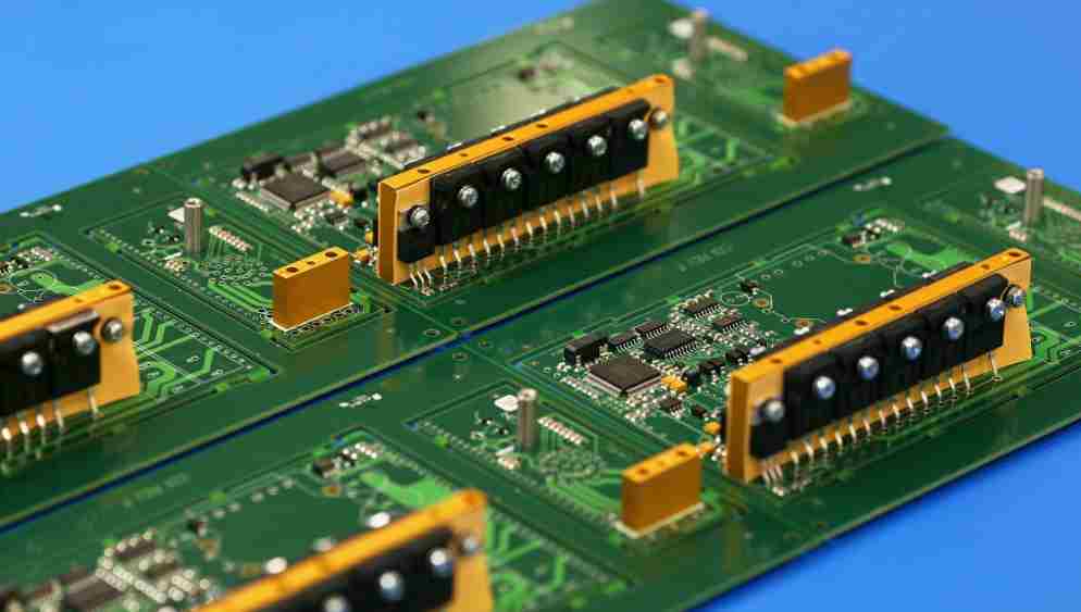
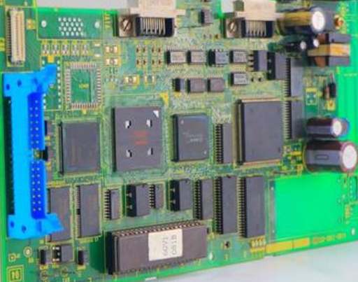
PCB board can be divided into single layer board, double layer board and multi layer board. Various electronic components are integrated on a PCB board. On the most basic single-layer PCB, the parts are concentrated on one side and the wires are concentrated on the other. In this way, we need to make holes in the board so that the connector can go through the board to the other side, so the connector of the part is welded to the other side. Because of this, the front and back of such PCB are respectively called parts (ComponentSide) and welding (SolderSide).
A double layer can be thought of as consisting of two single layers glued together, with electronic components and wiring on both sides. Sometimes it is necessary to connect a single wire from one side to the other side of the board through a pilot hole (via). A pilot hole is a small hole in a PCB filled with or coated with metal that can be connected to wires on both sides. Now many computer motherboards are using 4 or even 6 layers of PCB board, and graphics cards are generally in use of 6 layers of PCB board, many high-end graphics cards like nVIDIAGeForce4Ti series using 8 layers of PCB board, this is the so-called multi-layer PCB board. The problem of connecting the lines between the layers is also encountered on multilayer PCB boards, which can also be achieved through pilot holes.
Because the PCB is multilayer, sometimes the pilot holes do not need to penetrate the entire PCB. Such pilot holes are called Buriedvias and Blindvias because they only penetrate a few layers. Blind holes connect several layers of internal PCB to the surface PCB without penetrating the entire board. The buried hole is only connected to the PCB inside, so it is not visible from the surface. In multilayer PCB, the whole layer is directly connected to the ground wire and power supply. So we classify each layer as Signal layer, Power layer or Ground layer. If the parts on the PCB require different power supplies, usually the PCB will have more than two layers of power and wire. The more PCB layers used, the higher the cost. Of course, the use of more layers of PCB board to provide signal stability is very helpful.
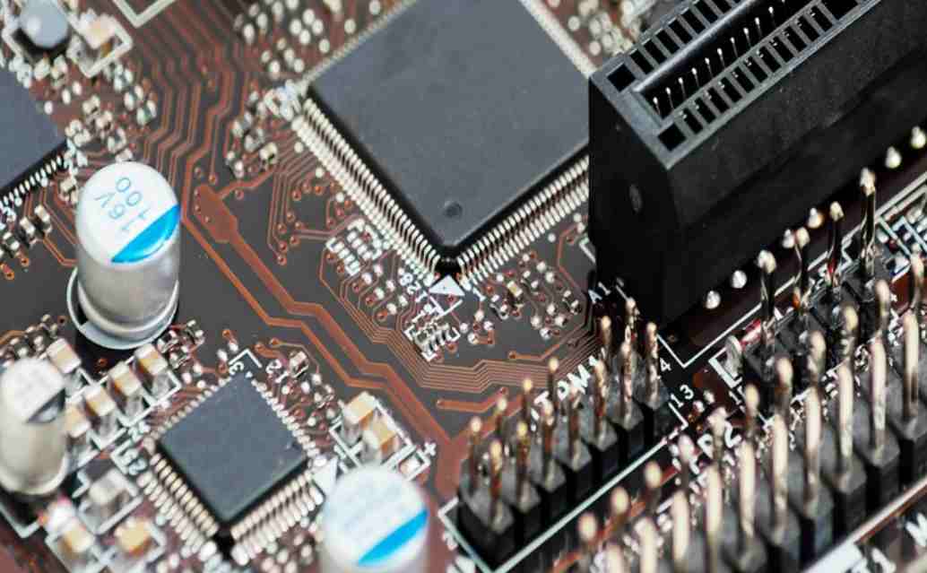
Professional PCB board production process is quite complex, take 4-layer PCB board as an example. The PCB of the main board is mostly 4 layers. During manufacturing, the middle two layers are first rolled, cut, etched, oxidized and electroplated respectively. The four layers are component surface, power layer, stratum and solder lamination. The 4 layers are then rolled together to form a PCB of the motherboard. Then punch holes and make holes. After cleaning, the outer two layers of line printing, copper coating, etching, testing, welding resistance layer, screen printing. Finally, the whole PCB (including many motherboards) is stamped into a PCB of the motherboard, and then the vacuum packaging is carried out after the test. If the copper coating is not well applied in the process of PCB production, there will be weak paste phenomenon, which is easy to hidden short circuit or capacitor effect (easy to produce interference). The holes on PCB must also be paid attention to. If the hole is not in the center, but to the side, it will cause uneven matching, or easy contact with the power layer or formation in the middle, resulting in potential short circuit or poor grounding factors.
Copper wiring process
The first step is to establish the wiring between the parts. We use negative transfer to express the working film on a metal conductor. The trick is to cover the entire surface with a thin layer of copper foil and remove any excess. Supplemental transfer is another less popular method, which is to apply copper wire only where it is needed, but we won't talk about that much here. Positive photoresists are made of photosensitive agents that dissolve under illumination. There are many ways to treat a photoresist on a copper surface, but the most common way is to heat it and roll it over a surface containing the photoresist. It can also be sprayed on top in liquid form, but dry film provides higher resolution and allows for thinner wires. The mask is just a template for the PCB layer in manufacture. Before the photoresist on the PCB board has been exposed to UV light, the cover on the top of the mask can prevent some areas of the photoresist from being exposed. These areas, covered by the photoresist, will become wiring. Other bare copper parts to be etched after photoresist development. The etching process can be done by dipping the board into an etching solvent or spraying the solvent onto the board. Generally used as an etching solvent using ferric chloride, etc. The remaining photoresist is removed after etching.
1. Wiring width and current
General width should not be less than 0.2mm (8mil)
On high density and high precision PCB, the spacing and line width are generally 0.3mm (12mil).
When the thickness of the copper foil is about 50um, the wire width is 1 ~ 1.5mm (60mil) = 2A
Common ground generally 80mil, more attention should be paid to applications with microprocessors.
2. How high frequency is high speed board?
When the signal's rising/falling edge time is 3~6 times the signal transmission time, it is considered to be a high-speed signal.
For digital circuits, the key is to look at the steepness of the edge of the signal, the time it takes to rise and fall,
According to a very classic book High Speed Digtal Design, the signal goes from 10% to 90% in less than 6 times wire delay, which is high speed signal! ------ that is! Even the 8KHz square wave signal, as long as the edge is steep enough, is still a high speed signal, and the transmission line theory needs to be used in wiring
3.PCB board stacking and layering
Four - ply plates have the following stacking sequences. The following are the advantages and disadvantages of different layers:
The first case
GND S1+POWER
S2+POWER
GND
Second case
SIG1
GND
POWER
SIG2
The third case
GND
S1
S2
POWER
Note: S1 signal wiring layer 1, S2 signal wiring layer 2; GND Ground POWER Power layer
The first case should be the best case of the four layers. Because the outer layer is the stratum, it has shielding effect on EMI, and the power layer is also close to the stratum reliably, which makes the internal resistance of the power supply smaller and achieves the best suburban fruit. But the first case can not be used when the board density is relatively high. Because then, you can't guarantee the integrity of the first layer, so the second layer gets worse. In addition, this structure can not be used in the case of high power consumption of the whole board.
The second scenario is the one we use most often. From the structure of the board, it is not suitable for high-speed digital circuit design. Because in this structure, it is difficult to maintain a low power impedance. Take a plate 2mm as an example: Z0=50ohm is required. The line width is 8mil. The copper foil is 35 replicas thick. So the signal is 0.14mm between the first layer and the ground. And the ground and power layer is 1.58mm. This greatly increases the internal resistance of the power supply. In this structure, because the radiation is to the space, need to add a shielding plate, in order to reduce EMI.
In the third case, the signal line on S1 is of the best quality. S2 comes second. It shields EMI. But the power impedance is larger. The board can be used for the whole board power consumption is high and the board is an interference source or close to the interference source.
4. Impedance matching
The amplitude of the reflected voltage signal is determined by the source reflection coefficient ρs and load reflection coefficient ρL
ρL = (RL-Z0)/(RL + Z0) and ρS = (Rs-Z0)/(RS + Z0)
In the above equation, if RL=Z0, the load reflection coefficient ρL=0. If RS=Z0 source reflection coefficient ρS=0.
Because the common transmission line impedance Z0 should usually meet the requirements of 50Ω about 50Ω, and the load impedance is usually in several thousand ohms to tens of thousands of ohms. Therefore, it is difficult to achieve impedance matching at the load end. However, because the signal source (output) impedance is usually relatively small, roughly ten ohm. Thus it is much easier to achieve impedance matching at the source. If the load is connected to a resistor, the resistor will absorb part of the signal, which is not good for transmission (my understanding). When the TTL/CMOS standard 24mA drive current is selected, the output impedance is approximately 13Ω. If the line impedance is Z0=50Ω, then a 33Ω source matching resistance should be added. 13Ω+33Ω=46Ω (approximately 50Ω, weak underdamping helps the setup time of the signal)
When other transmission standards and drive currents are selected, the matching impedance will differ. In high-speed logic and circuit design, for some key signals, such as clock, control signals, we recommend that we must add source matching resistance.
In this way, the signal will be reflected back from the load, because the source impedance matches, the reflected signal will not be reflected back.


Достаточно загрузить файлы Gerber, BOM и проектные документы, и команда KINGFORD предоставит полное предложение в течение 24 часов.