
Контрактное производство электроники под ключ в Китае
Шэньчжэнь, район Баоань, улица Фуюн, улица Фуцяо, район 3, промышленный парк Лонгхуй 6

PCB design engineers need to master a wide range of knowledge system, including electrical theory, component performance, digital circuit and analog circuit, PCBA processing process and DFM manufacturability theory, welding practice, schematic drawing and Layout, single-chip logic and basic principles.
1. If the designed circuit system includes FPGA devices, Quartus II software must be used to verify pin allocation before schematic drawing. Some special pins in FPGA cannot be used as normal IO.
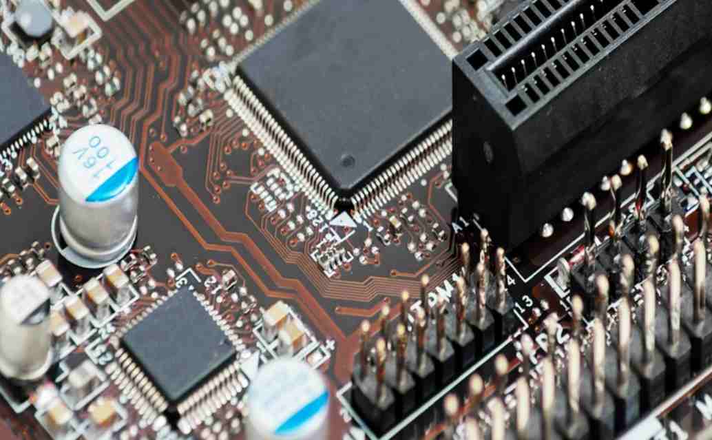
2, 4 layers board from top to bottom: signal plane layer, ground, power supply, signal plane layer; The six layers from top to bottom are: signal plane layer, ground, signal internal electrical layer, signal internal electrical layer, power supply, signal plane layer. For boards with more than 6 layers (advantages are: anti-interference radiation), the internal electrical layer is preferred to be routed. If not, the plane layer is selected, and the ground or power layer is prohibited to be routed (cause: the power layer will be divided, resulting in parasitic effect).
3, multi-power system wiring: such as FPGA+DSP system to do 6 layers of board, generally at least 3.3V+1.2V+1.8V+5V.
3.3V is generally the main power supply, directly lay the power layer, through the hole is easy to distribute the global power network;
5V May be a power input, and only copper is needed in a small area. And as thick as possible.
1.2V and 1.8V are the core power supply (if directly connected by wire will encounter great difficulties in the face of BGA devices), the layout should be separated from 1.2V and 1.8V as far as possible, and the components connected within 1.2V or 1.8V are arranged in a compact area and connected by copper
In short, because the power network is spread over the entirePCB board, it would be complicated to use the wiring method and it would take a long way around, so using the copper coating method is a good choice!
4. The crossing mode is adopted between adjacent layers: it can not only reduce the electromagnetic interference between parallel wires, but also facilitate the wiring.
5, analog digital to isolation, how isolation method? The layout will be used for analog signal devices and digital signal devices separate, and then cut from the middle of the AD chip!
The analog signal is laid on the analog ground, and the analog ground/analog power supply and the digital power supply are connected through a single point of inductance/magnetic beads.
6. PCB design based on PCB design software can also be regarded as a software development process. Software engineering pays most attention to the idea of "iterative development" to reduce the probability of PCB errors.
(1) schematic check, especially pay attention to the power supply and ground of the device (power supply and ground are the blood of the system, can not be the slightest neglect);
(2) PCB packaging and drawing (confirm whether the pins in the schematic diagram are wrong);
(3) After confirming the PCB packaging size one by one, add verification labels to the packaging library of this design;
(4) Import the netlist, and adjust the sequence of signals in the schematic diagram while laying out (OrCAD component automatic numbering function cannot be used after laying out).
In the specific design process, the basic knowledge to be mastered includes:
1. Preliminary preparation
This includes preparing component libraries and schematics. Before the PCB design, the schematic SCH component library and PCB component packaging library should be prepared first.
The PCB component package library should preferably be built by the engineer based on the standard dimension data of the selected component. In principle, first build PC component packaging library, and then build schematic SCH component library.
PCB component package library has high requirements, which directly affects the installation of PCB. Schematic SCH component library requirements are relatively loose, but care should be taken to define pin attributes and correspondence with PCB component packaging library.
2. PCB structure design
According to the determined size of the circuit board and various mechanical positioning, PCB board frame is drawn in the PCB design environment, and the required connectors, keys/switches, screw holes, assembly holes and so on are placed according to the positioning requirements.
Fully consider and determine wiring and non-wiring areas (e.g., how much of the area around screw holes is non-wiring).
3. PCB layout design
Layout design is to place components in the PCB board frame according to the design requirements. Generate the network table (Design→CreateNetlist) in the schematic tool, and then import the network table (Design→ImportNetlist) in the PCB software. After the network table is successfully imported, it will exist in the software background. All the devices can be called out by the Placement operation, and there is a flying line between the pins. Then the device layout design can be carried out.
PCB layout design is the first important process in the whole PCB design process. The more complex PCB board is, the better or worse the layout will directly affect the difficulty of the realization of the wiring later.
The layout design depends on the circuit foundation and design experience of circuit board designers, which is a higher level of requirements for circuit board designers. Junior circuit board designers are inexperienced, suitable for small module layout design or PCB layout design task with low difficulty of whole board.
4. PCB routing design
PCB routing design is the most workload process in the whole PCB design, which directly affects the performance of PCB board.
In the design process of PCB, wiring generally has three levels:
The first is the cloth, which is the most basic entry requirements of PCB design;
The second is to meet the electrical performance, which is to measure whether a PCB board qualified standard, after the line layout, carefully adjust the wiring, so that it can achieve the best electrical performance;
Again is neat and beautiful, disorderly wiring, even if the electrical performance clearance will also bring great inconvenience to the later board optimization and testing and maintenance, wiring requirements neat and uniform, can not criss-cross without rules.
5. Wiring optimization and silk-screen placement
"PCB design is not the best, only better", "PCB design is a defective art", mainly because PCB design to achieve all aspects of hardware design requirements, and individual requirements may be conflicting, you can not have your cake and eat it.
For example, a PCB design project needs to be designed as a 6-layer board after evaluation by the circuit board designer, but the product hardware needs to be designed as a 4-layer board due to cost consideration, so the signal shielding layer can only be sacrificed, which leads to the increase of signal crosstalk between adjacent wiring layers and the decrease of signal quality.
A general rule of thumb for design is to optimize the wiring twice as long as the initial wiring. After PCB routing optimization is complete, post-processing is required. The main processing is the silk screen logo on the PCB board surface. During the design, the characters in the bottom layer of the silk screen must be mirrored to avoid confusion with the top layer of the silk screen.
6. Check the network DRC and structure
Quality control is an important part of PCB design process. General quality control means include: design self-inspection, design mutual inspection, expert review meeting, special inspection, etc.
Schematic diagram and structural element diagram are the most basic design requirements. Network DRC inspection and structural inspection are to confirm that PCB design meets the two input conditions of schematic diagram netlist and structural element diagram respectively.
Generally, circuit board designers have their own accumulated design quality Checklist, in which some items are based on company or department specifications and some are based on their own experience. Special inspection includes design Valor inspection and DFM inspection. These two parts focus on PCB design output back-end processing light drawing files.
7, PCB board
Before the PCB is formally processed into the board, the circuit board designer needs to communicate with the PE of the PCB plate supplier factory to reply the manufacturer's confirmation questions about PCB board processing.
This includes but is not limited to: PCB board type selection, line width and line distance adjustment, impedance control adjustment, PCB stacking thickness adjustment, surface treatment processing technology, aperture tolerance control and delivery standards.


Достаточно загрузить файлы Gerber, BOM и проектные документы, и команда KINGFORD предоставит полное предложение в течение 24 часов.