
Контрактное производство электроники под ключ в Китае
Шэньчжэнь, район Баоань, улица Фуюн, улица Фуцяо, район 3, промышленный парк Лонгхуй 6

Not all products with fewer or smaller components are cheaper. Just like chips at this stage, the smaller the area, the more expensive it actually is. PCB board is the same, it does not mean the thinner the cheaper, the same layer, the lower the cost.
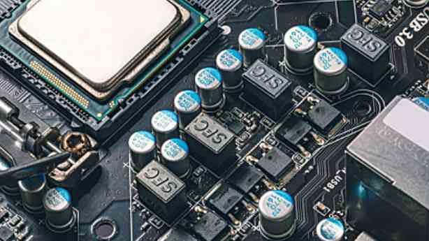
The circuit board has two different structures: core structure and foil structure.
In the core structure, all the conductive layers in the circuit board are coated on the core material; In the foil-coated structure, only the internal conductive layer of the circuit board is applied to the core material, and the external conductive layer is applied to the foil dielectric plate. All conductive layers are bonded together by a medium using a multilamination process.
Nuclear material is double-sided foil in a factory. Because each core has two sides, the PCB has an even number of conductive layers when fully utilized. Why not use foil on one side and nuclear structure on the rest? The main reasons are: the cost of PCB and PCB bending degree.
Cost advantage of even layer circuit boards
Because there is one less layer of medium and coating foil, the cost of odd-numbered PCB board raw materials is slightly lower than that of even-numbered PCB board. However, the processing cost of odd-numbered layer PCB is obviously higher than that of even-numbered layer PCB. However, the foil/core structure significantly increases the processing cost of the outer layer.
Odd layer PCB needs to add non - standard laminated core layer bonding technology on the basis of nuclear structure technology. Compared with the nuclear structure, the production efficiency of the plant adding foil outside the nuclear structure will decrease. Prior to laminating, the outer core requires additional processing, which increases the risk of scratches and etching errors on the outer layer.
Seeing the above content, I believe many people should understand that the actual PCB board does not mean that the thinner it is, the cheaper it is. It is defined according to different products. Perhaps a product will be much cheaper after reducing the area or cost, but electronic products as technical products, its function is still very different.
Can not be ignored PCB design details
PCB is printed circuit board, is the carrier of electronic circuit. In modern electronic products, almost all need to use PCB. PCB design is a link behind the circuit design, but also to the principle of the circuit redesign. Some new engineers tend to underestimate the importance of PCB design and leave this tedious and laborious task to technicians. Here I will tell you a story about PCB design.

Ordinary touch-tone telephone, in fact, is not what high-tech products, compared with the early dial electronic telephone, it adds a piece of dual audio/pulse dial control integrated circuit in the circuit, some products also increase the hands-free call function, users use the phone, if you press the hands-free button, without picking up the phone, you can hear or put out. People who are familiar with the principle of phone circuit know that the hands-free circuit is composed of "automatic receive/send control circuit" and "audio power amplifier circuit". These circuits are implemented by special IC. There is no need for innovative design in principle.
The phone sales plan was delayed for many years. Later, it was found that the cause of the wrong triggering of hands-free was the PCB design of the circuit. Later, the company's phone products were required to change the hands-free buttons to mechanical buttons, so as to obtain the network access permit of telecom. The direct economic loss caused by this incident to the enterprise is more than tens of millions of yuan.
Some designers think that PCB design is simple labor, using PROTEL or other software tools, through automatic layout, automatic wiring, can be completed. Single panel can not be spread through, use double panel, no longer use multilayer board, or set jumper, short jumper is not long jumper, no longer use jumper, always can be spread through.
And I know an old engineer, they design PCB in the early days before the use of computers, still can complete the circuit PCB design containing hundreds of thousands of components. And their design of the PCB, layout and wiring are quite neat, jumper, cross line very few, the original components arranged orderly and reasonable, and meet the requirements of the process specification. We see the early domestic black and white TV PCB, belongs to their era of engineers masterpiece.
Although later on when I was designing PCBS, I used a computer. However, I still think that these old engineers must have some tricks to learn from in PCB design. It is hard for our young engineers to imagine how they used to complete complex PCB design with pencil and chequered paper. Indeed, I also gained a lot of experience from him, such as: how to arrange the components can be easily routed, how to effectively use the board space under the dual-in-line IC, how to plan the layout as much as possible before wiring and so on.
My own experience is: PCB design, not only technology, but also art, art involves a lot of subjective factors, so engineers should also pay attention to improve their own culture.
The tool helps us do a lot of hard work, but what it does automatically doesn't work well for every product. Because it helps us to complete the product design is common and general side, not automatically complete the product optimization surface design, for example: the use of PROTEL or other software tools, through automatic layout, automatic wiring, can be completed just the usual connection, from a certain point of view is just to connect the device together. Therefore, to really design a pcb of a product, more designers are specific to the situation of the product and analysis, so as to complete a very unique design.
What is PCB half hole plate?
2023-04-22


Достаточно загрузить файлы Gerber, BOM и проектные документы, и команда KINGFORD предоставит полное предложение в течение 24 часов.