
Контрактное производство электроники под ключ в Китае
Шэньчжэнь, район Баоань, улица Фуюн, улица Фуцяо, район 3, промышленный парк Лонгхуй 6

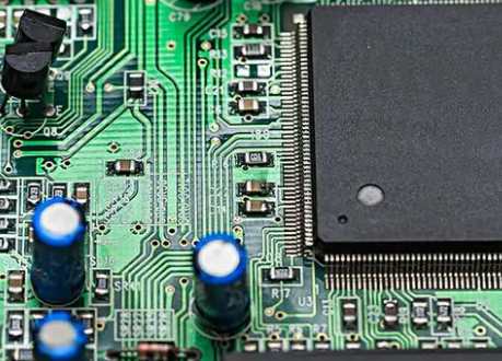
In the 4G era, PCBS are mainly used in base station Bbus (base station backplane, base station board) and RRU hung under the antenna. Due to the small size of RRU, PCB demand is relatively small. In the era of 5G, base station antennas evolve from passive to active, and RRU and antenna are merged into active antenna units (AAU) that support large-scale antennas and have higher requirements for antenna integration. FPGA chips, optical modules, RF components and power systems will be integrated into PCB boards that support high speed and high frequency. The structural changes of 5G antenna radio frequency combined with a substantial increase in the number of 5G base stations, bringing new opportunities for PCB communication.
According to the quantitative calculation of 5G PCB market space, the high frequency and high speed PCB space is huge. We take 1 5G Acer station BBU connected with 3 AAU as an example to calculate, and the PCB value of a single Acer station is about 22,641 yuan, about 3.4 times that of 4G. The value of high-frequency CCL in a single 5G macro base station is about 2430 yuan/station, about 11.5 times that of 4G. In addition, the market space of PCB and high-frequency CCL is calculated according to the 10% annual price reduction: the market space of 5G base station PCB is about 88.7 billion yuan, 2.2 times as elastic as that of 4G; the market space of high-frequency CCL is about 9.53 billion yuan, 7.5 times as elastic as that of 4G.
High frequency and high speed PCB technology barriers, domestic replacement space is huge high frequency and high speed PCB put forward higher requirements for materials, need low dielectric constant, low loss factor substrate, surface roughness smaller copper foil, and low loss factor solder resistance ink. Due to high technical barriers, high frequency and high speed copper clad plate is mainly monopolized by Rogers, Yaron and other overseas manufacturers, accounting for more than 90% of the high frequency plate market share, among which Rogers exclusively occupies more than 40% of the market share, domestic substitution space is huge, and the manufacturers taking the lead in the domestic industrial chain are expected to benefit.
With the full opening of 5G base station construction in 2019, the market space of high-frequency and high-speed PCB is expected to accelerate.
It is suggested to focus on Shennan Circuit, Shanghai Electric (002463) and Dongshan Precision (002384), the leading domestic communication PCB companies that have cooperated with mainstream communication equipment manufacturers. In addition, as high frequency and high speed PCB puts forward higher requirements on materials, requiring substrate with low dielectric constant and low loss factor, copper foil with smaller surface roughness, and welding resistance ink with low loss factor, it is suggested to pay attention to the industry chain related manufacturers that have made positive progress in the upstream raw material field of the industry and have the ability to substitute high frequency and high speed CCL domestically.
The difference between positive and negative PCB circuit boards
Negative film of PCB circuit board: Generally, it is the tenting process we talk about. The drug solution used is acidic etching negative film because after the negative is made, the line or copper surface is transparent, and the part is not black. After exposure through the line process, the transparent part is hardened by chemical action due to the dry film resistance agent under light, and the following development process will not be hardened In the etching process, only the copper foil (the black part of the negative) is eroded, while the dry film is not washed off and belongs to the line we want (the transparent part of the negative).

PCB circuit board positive film: generally we talk about the pattern process, the use of liquid for alkaline etching positive film if the negative, to the line or copper surface is black, and do not part of the transparent, the same through the line process exposure, transparent part due to dry film resistance by light chemical hardening, the next development process will not harden dry The film is washed off, followed by the tin lead plating process. The tin lead is plated on the copper surface where the dry film was washed off in the previous process (developing), and then the film is removed (removing the dry film hardened by light). In the next process etching, the copper foil without the tin lead protection is bitten off with an alkaline solution (the transparent part of the negative), and the remaining line is what we want (the black part of the negative).
Positive and negative film is actually according to the company's process to choose, positive: process is (double panel) opening - drilling -PTH (a plating also called thickened copper) - line - two copper (graphic plating) and then go SES line (film - etching - tin) negative film: Process is (double panel) opening - drilling -PTH(a plating also called thickening copper) - line (without two copper graphic plating) and then go DES line (etching - film)
(1) To distinguish the film (negative) parent film, working film, positive and negative film surface: film has parent film and working film (sub-film), black film and yellow film, positive film and negative film;
② Generally speaking, the mother film for black film, also known as silver salt tablet, is mainly used to copy the work film (yellow film is also known as diazo tablet), but the work film is not necessarily only yellow, there are also black pieces to do the work film, which is mainly to do high precision HDI board or in order to save money in a one-time small batch circuit board production, Yellow tablets are used in the manufacture of ordinary boards and ordinary circuit boards.
(3) When the drug film surface is differentiated, the smooth surface of the black film is the drug film, and the yellow film is on the contrary. Generally, it can be seen that the side is the drug film surface by scraping the pen or blade on the film. (Parent: positive character positive medicine face, child: positive character negative medicine face)
(4) Note when using yellow tablets: there are two kinds of smooth surface and dumb surface, and the second kind is easy to appear oil surface indentation when using.
(5) Film line (with copper) on the negative light, light is positive; Positive for the use of graphic plating, development is off the line, leaving the role of corrosion resistance plating, the main plating is lead tin. The negative film is used for direct etching, and the corrosion resistance left after development is a circuit, which is etched directly with acid etching solution.


Достаточно загрузить файлы Gerber, BOM и проектные документы, и команда KINGFORD предоставит полное предложение в течение 24 часов.