
Контрактное производство электроники под ключ в Китае
Шэньчжэнь, район Баоань, улица Фуюн, улица Фуцяо, район 3, промышленный парк Лонгхуй 6

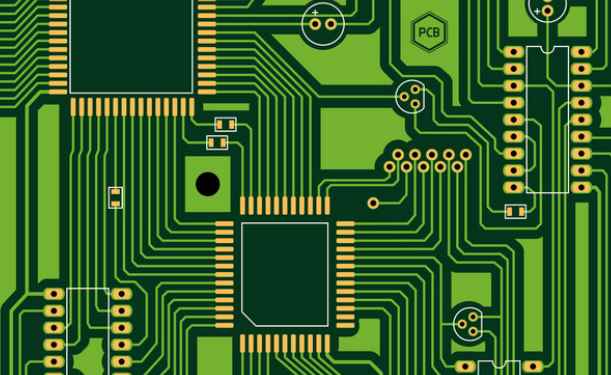
PCB boardin the process of design and production will always encounter a variety of problems, such as PCB board short circuit, PCB board dark and granular contact, board bending. In this article, Xiaobian and everyone together to understand some of the common causes of poor PCB board.
PCB short circuit
This is one of the common faults that directly cause the PCB board to fail to work, and there are many reasons for this problem, we will analyze one by one below.
1) The biggest cause of PCB short circuit is improper design of welding pad. In this case, the circular welding pad can be changed to oval shape to increase the distance between points to prevent short circuit.
2) Improper design of PCB parts direction will also cause the board short circuit, unable to work. Such as SOIC feet if parallel to the tin wave, it is easy to cause short circuit accident, at this time can be appropriate to modify the direction of the parts, so that it is perpendicular to the tin wave.
3) There is another possibility that will cause short circuit fault of PCB, that is, automatic plug-in foot bending. As IPC stipulates that the length of the pin is less than 2mm and the parts will fall off when the Angle of the foot is too large, it is easy to cause short circuit. It is necessary to leave the solder joint more than 2mm away from the line.
In addition to the three reasons mentioned above, there are also some reasons that will lead to short circuit fault of PCB board, such as too large holes in the substrate, low temperature of the tin furnace, poor weldability of the board surface, failure of welding resistance film, pollution of the board surface, etc., are relatively common fault causes. Engineers can compare the above reasons and the occurrence of faults one by one to eliminate and check.
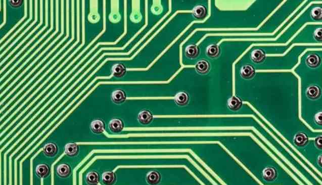
PCB open circuit
An open circuit occurs when the trace breaks, or when the solder is only on the pad and not on the component lead. In this case, there is no adhesion or connection between the component and the PCB. Like short circuits, these can occur during production or welding and other operations. Vibrating or stretching circuit boards, dropping them, or other mechanical deformation factors can damage the trace or solder joints. Similarly, chemical or moisture can cause solder or metal parts to wear out, which can cause component leads to break.
Dark and granular contacts appear on the PCB board
PCB board dark or into small granular contact problem, mostly due to solder pollution and dissolved tin mixed with too much oxide, the formation of solder joint structure is too brittle. Care should be taken not to confuse the dark color with the use of solder with low tin content.
Another reason for this problem is that the composition of the solder used in the process of processing and manufacturing changes, and the impurity content is too much. It is necessary to add pure tin or replace solder. Physical changes in stained glass fibre-deposition, such as separation between layers. But this situation is not bad solder joint. The reason is that the substrate is heated too high, need to reduce the preheating and solder temperature or increase the substrate travel speed.
PCB solder joints turn golden
In general, the solder of PCB board is silver gray, but occasionally there are golden solder joints. The main reason for this problem is that the temperature is too high. At this time, we only need to lower the temperature of the tin furnace.
Bad boards are also affected by the environment
Due to the structure of PCB itself, it is easy to cause damage to PCB board when in an unfavorable environment. Extreme temperature or temperature fluctuation, excessive humidity, high intensity vibration and other conditions are leading to board performance reduction or even scrap factors. For example, changes in ambient temperature can cause the board to deform. This will break the solder joints, bend the shape of the board, or it may cause the copper thread on the board to break.

Buried, blind, through hole technology
The combination of buried, blind and through hole technology is also an important way to improve the density of printed circuits. Generally, buried and blind holes are small holes, in addition to improving the number of wiring on the board, buried and blind holes are used "recently" interlayer interconnection, greatly reducing the number of through holes, isolation disk Settings will be greatly reduced, thus increasing the number of effective wiring and interlayer interconnection in the board, improve the interconnection density.
Therefore, the interconnect density of the buried, blind and through hole combined multilayer board is at least 3 times higher than that of the conventional all-through hole plate structure under the same size and number of layers. If the printed board combined with buried, blind and through hole is under the same technical index, its size will be greatly reduced or the number of layers will be significantly reduced.
Therefore, in the high density surface mounted printed board, buried and blind hole technology has been increasingly applied, not only in the large computer, communication equipment and other surface mounted printed board, but also in the civil, industrial field has been widely used, even in some thin plate has also been applied. Such as the PCMCIA, Smard, IC card and other thin six layers of the board.
Buried, blind hole structure of the printed circuit board, generally use the "sub-board" production mode to complete, which means that after several times of pressing plate, drilling, hole plating and so on to complete, so precise positioning is very important.
On the other hand, moisture in the air can cause oxidation, corrosion and rust on metal surfaces, such as exposed copper wires, solder joints, pads and component leads. Accumulation of dirt, dust, or debris on the surface of components and circuit boards can also reduce air flow and cooling of components, leading to overheating and performance degradation of the PCB. Vibration, dropping, hitting or bending the PCB will deform and lead to initial cracks, while high current or overvoltage will lead to breakdown of the PCB board or lead to rapid aging of components and pathways.
Why is the common PCB board thickness 1.6mm
2023-03-29


Достаточно загрузить файлы Gerber, BOM и проектные документы, и команда KINGFORD предоставит полное предложение в течение 24 часов.