
Контрактное производство электроники под ключ в Китае
Шэньчжэнь, район Баоань, улица Фуюн, улица Фуцяо, район 3, промышленный парк Лонгхуй 6

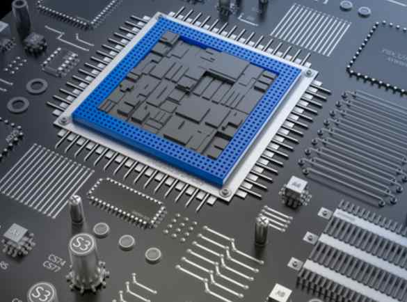
SMT patch is short for a series of processes based on PCB. PCB (printed circuit board) means printed circuit board.
SMT (short for Surface Mounted Technology) is a popular technology and process in the electronic assembly industry. Surface Mount Technology (SMT) of electronic circuits is called surface mount or surface mount technology. It is a kind of pin-free or short-lead surface assembly components (SMC/SMD, Chinese known as chip components) installed on the Printed Circuit Board (PCB) surface or other substrate surface, through reflow welding or immersion welding and other methods to be welded and assembled circuit installation technology.
Under normal circumstances, the electronic products we use are made of pcb plus a variety of capacitors, resistors and other electronic components designed according to the circuit diagram, so the shape of the electrical appliances need a variety of different SMT patch processing technology to process.
SMT basic process elements: solder paste printing -> Parts mounting --> Reflow welding --> AOI Optical Detection --> Maintenance --> The board is divided.
Some people may ask why it is so complicated to connect an electronic component. In fact, this is closely related to the development of our electronic industry. Nowadays, electronic products pursue miniaturization, and the previously used punch plug-in components can not be reduced. The function of electronic products is complete, the integrated circuit (IC) used has no perforated components, especially large scale, high integration IC, have to use surface patch components. Product mass, production automation, the factory to low cost and high output, produce products to meet customer needs and strengthen the market competitiveness of the development of electronic components, integrated circuit (IC) development, semiconductor materials of multiple applications. Electronic science and technology revolution is imperative, the pursuit of the trend. It can be imagined that the development of smt surface assembly technology and technology is inevitable in the case that intel,amd and other manufacturers of cpu and image processing devices have improved their production process to more than 20 nanometers.
smt patch processing advantages: high assembly density, small size of electronic products, light weight, the size and weight of the patch components is only about 1/10 of the traditional plug-in components, generally after the adoption of SMT, the size of electronic products reduced by 40%~60%, 60%~80% weight reduction. High ** ** ability, strong vibration resistance. Low defect rate of solder joint. Good high frequency characteristics.
Electromagnetic and radio frequency interference is reduced. Easy to realize automation, improve production efficiency. Reduce the cost by 30%~50%. Save materials, energy, equipment, manpower, time, etc.
It is precisely because of the complex technological process of smt patch processing that there are many smt patch processing factories. In Shenzhen, thanks to the booming development of the electronic industry,smt patch processing has achieved a prosperity of the industry.

Chip heating
This is mainly for high voltage driver chips with built-in power modulators. If the current consumed by the chip is 2mA, 300V voltage is applied to the chip, and the power consumption of the chip is 0.6W, of course, it will cause the heat of the chip. The large current of the driver chip comes from the consumption of the driving power MOS tube. The simple calculation formula is I=cvf.
Considering the resistance benefit of charging, the actual I=2cvf, where c is the cgs capacitance of the power MOS tube and v is the gate voltage when the power tube is switched on. Therefore, in order to reduce the power consumption of the chip, try to reduce c, v and f. If c, v, f cannot be changed, then please find a way to distribute the power of the chip to the off-chip device. Be careful not to introduce additional power consumption. Another simple point is to consider the best heat dissipation.
Power tube heating
The power consumption of power tube is divided into two parts, switching loss and on-off loss. Note that most occasions, especially LED mains drive applications, switch damage is far greater than the on-off loss. The switching loss is related to the cgd and cgs of the power tube as well as the driving capacity and working frequency of the chip, so the heating of the power tube can be solved from the following aspects:
01. MOS power tube can not be selected unilaterally according to the size of the on-off resistance, because the smaller the internal resistance, the larger the capacitance of cgs and cgd.
For example, cgs for 1N60 is about 250pF, 2N60 cgs is about 350pF, 5N60 cgs is about 1200pF, the difference is too big, when choosing a power tube, enough is enough.
02, the rest is frequency and chip drive capability, here only talk about the effect of frequency. Frequency is also proportional to conduction loss, so when the power tube heating, * to think about whether the frequency selection is a little high. Find a way to lower the frequency!
However, it should be noted that when the frequency decreases, in order to obtain the same load capacity, the peak current must be increased or the inductance must also be increased, which may lead to the inductance entering the saturation region. If the inductance saturation current is large enough, you can consider changing CCM (continuous current mode) to DCM (discontinuous current mode), so you need to add a load capacitor.
Operating frequency drops
This is also a common phenomenon in the process of debugging, frequency reduction is mainly caused by two aspects. The input voltage and load voltage ratio is small, the system interference is large. For the former, be careful not to set the load voltage too high, although the load voltage is high, the efficiency will be high. For the latter, try the following:
1. Set the small current lower;
2. Clean wiring, especially the critical path of sense;
3. Select a small inductance or the inductance of a closed magnetic circuit;
4. Add RC low-pass filtering. The effect is a little bad. The consistency of C is not good and the deviation is a little large, but it should be enough for lighting.
There is no upside to downscaling anyway, only downside, so be sure to fix it.
Choice of inductor or transformer
With the same drive circuit, the inductance produced by a has no problem, and the inductance current produced by b becomes smaller. In this case, look at the inductive current waveform. Some do not notice this phenomenon, directly adjust the sense resistance or working frequency to reach the required current, which may seriously affect the service life of LED.
Therefore, before the design, reasonable calculation is perfect, if the theoretical calculation parameters and debugging parameters are a little far away, to consider whether the frequency reduction and transformer saturation. When the transformer is saturated, L will become smaller, resulting in a sharp rise in the peak current increment caused by transmission delay, so the peak current of LED will also increase. If the average current stays the same, you can only watch the light fade.

LED current size
2023-03-26


Достаточно загрузить файлы Gerber, BOM и проектные документы, и команда KINGFORD предоставит полное предложение в течение 24 часов.