
Контрактное производство электроники под ключ в Китае
Шэньчжэнь, район Баоань, улица Фуюн, улица Фуцяо, район 3, промышленный парк Лонгхуй 6

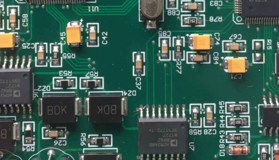
Whether in the manufacturing and assembly process or in actual use, PCB to have reliable performance, this is very important. So, what specific measures need to be implemented in the production of high reliability PCB circuit boards?
1, 25 micron hole wall copper thickness
Benefits: Enhanced reliability, including improved Z-axis expansion resistance.
Risks of not doing so: blowing or degassing, electrical connectivity problems during assembly (inner separation, hole wall breakage), or the possibility of failure under load conditions in actual use.
2. No welding repair or line repair
Benefits: Perfect circuit ensures reliability and safety, no maintenance, no risk
Risk of not doing this: If not repaired properly, the circuit board will be disconnected.
3. Exceed the cleanliness requirements of IPC specifications
Benefits: Increased PCB board cleanliness improves reliability.
Risks of not doing this: Residue, solder buildup on the circuit board poses a risk to the solder shield, which can lead to reliability issues (poor solder joints/electrical failures).
4, strictly control the service life of each kind of surface treatment
Benefits: Solderability, reliability, and reduced risk of moisture intrusion
Risks of not doing so: The possibility of solderability problems due to the surface treatment of the older circuit boards can lead to delamination, inner layer and hole wall separation (circuit breaker) during assembly and/or actual use.
5. Copper clad plate tolerance meets the requirements of IPC4101ClassB/L
Benefits: Strict control of dielectric layer thickness, reduce electrical performance expected value deviation.
Risks of not doing so: Electrical performance may not be up to the specified requirements, and the output/performance of the same batch of components may vary greatly.
6. Define solder resistance materials to ensure compliance with IPC-SM-840ClassT requirements
Benefits: Achieve ink safety and ensure that the solder resistance layer ink meets UL standards.
Risks of not doing so: Poor quality ink can lead to adhesion, flux resistance and hardness problems.
7. Define tolerances for shapes, holes and other mechanical features
Benefits: Strict tolerance control can improve the dimensional quality of the product - improve fit, shape and function
Risk of not doing this: Assembly problems, such as alignment/fit.
8. NCAB specifies the solder shield thickness, although IPC does not specify it
Benefits: Improved electrical insulation, reduced risk of flaking or loss of adhesion, enhanced resistance to mechanical impact.
Risks of not doing so: A thin solder shield can cause problems with adhesion, flux resistance and hardness.
9. Appearance requirements and repair requirements are defined, although IPC does not
Benefits: In the PCB manufacturing process carefully care and carefully cast safety.
Risks of not doing so: In addition to the visible problems, what are the invisible risks, as well as the impact on the assembly, and the actual use of the risk is difficult to predict.
10. Requirements for the depth of the plug hole
Benefits: High quality plugs will reduce the risk of failure during assembly.
Risk of not doing so: Chemical residue from the gold deposition can remain in the hole where the hole is not plugged, causing problems such as solderability. Moreover, tin beads may be hidden in the hole, causing a short circuit.


Достаточно загрузить файлы Gerber, BOM и проектные документы, и команда KINGFORD предоставит полное предложение в течение 24 часов.