
Контрактное производство электроники под ключ в Китае
Шэньчжэнь, район Баоань, улица Фуюн, улица Фуцяо, район 3, промышленный парк Лонгхуй 6

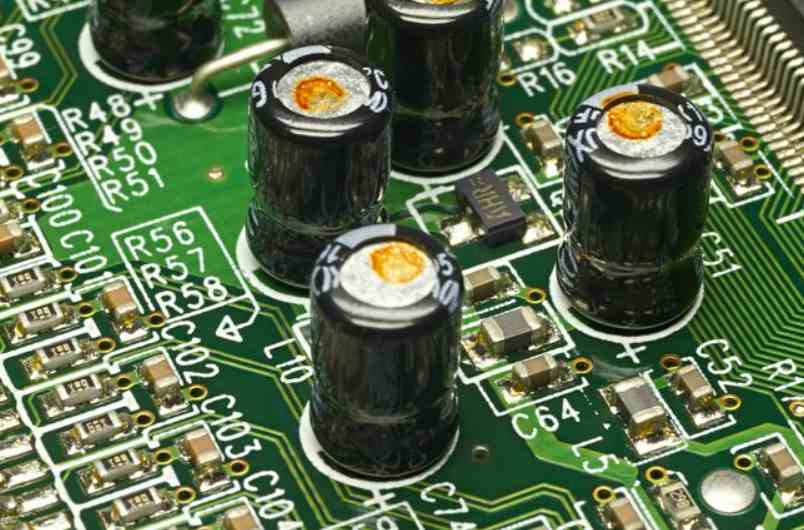
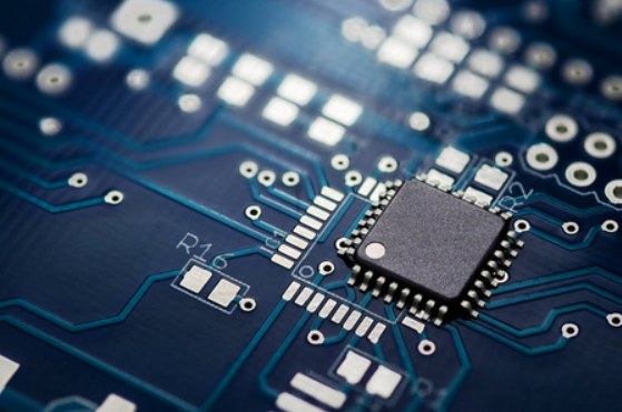
PCB inspection has the status of "account in the three armies" for PCB process quality, and is also the core competitive field of PCB manufacturers. It plays a fundamental role in the whole PCBA processing process. At present, the main PCB detection technologies at home and abroad can be divided into two categories: Optical Inspection and Electrical Inspection, Specifically, it includes PCB manual visual Inspection, PCB online inspection (ICT), PCB functional inspection (FCT), PCB active optical inspection (AOI), PCB active X-ray inspection (AXL, Automatic X-ray Inspection) and PCB laser inspection, a total of 6 kinds of detection technologies.
1. PCB manual visual inspection
The main magnifying glass or microscope is used to manually identify the short circuit, open circuit and some appearance defects on the PCB circuit board, such as foaming, distortion and so on
Advantage: Cost economy
Disadvantages: poor error correction rate and great subjective deviation. With the line width and line distance becoming narrower, this method has been gradually eliminated
2. PCB Online Testing (ICT)
The principle of ICT detection is mainly to simulate the electrical connection of the circuit board, so as to detect the main defects of PCB board such as open circuit and short circuit through the test point. ICT includes several testing devices such as Bed of Nails Tester and Flying Probe Tester.
Advantages: Low testing cost, easy programming, high defect coverage
Disadvantages: It is necessary to make special test fixture for PCB, which is relatively costly and difficult to use
3. PCB function Test (FCT)
Functional testing is mainly to simulate the use of products, the circuit board through professional equipment connection, programming, so as to truly reproduce the performance of the product in the process of use.
Advantage :100% ready to reproduce PCB performance
Disadvantages: Complicated design process, high cost, not suitable for most PCB production processes
4, PCB active optical detection (AOI)
Optical detection technology is relatively common and mature at present. It is mainly based on optical principle, combined with computer and automatic control method, to take pictures of PCB board graphics and compare them with preset images and programs, so as to detect problems in PCB board circuit connection very accurately.
Advantage: The detection success rate is extremely high
Disadvantages: The cost advantage is not very prominent, the efficiency is moderate, generally need to equip a large number of testing equipment to cope with mass production
5. PCB active X-ray detection
X-ray detection is mainly used in high-precision and difficult processes, such as BGA and PoP process design. Its principle is to detect the internal defects of PCB board through X-ray projection, similar to artificial X-ray film. It has good detection ability for blind holes and other processes.
Advantage: Adaptability to difficult tests
Disadvantages: high cost, poor detection efficiency and high repair cost
6, PCB laser detection
The principle is to use a laser beam to scan PCB, collect all the measured data, and compare the data with the preset limit value of the system, and accurately feedback the deviation between the circuit board and the design on the data level, so as to accurately find the defects.
Advantages: Suitable for mass production, high speed, independent of fixture
Disadvantages: High initial cost, maintenance and programming requires professionals
PCB detection technology changes with each passing day, mainly in efficiency, accuracy and cost to find a balance, there are a lot of detection equipment in the market, applied to different occasions, detection of basic short circuit and circuit opening defects is more handy. However, any PCB detection technology cannot be separated from human management.
What does SMT mean?
2023-03-04


Достаточно загрузить файлы Gerber, BOM и проектные документы, и команда KINGFORD предоставит полное предложение в течение 24 часов.