
Контрактное производство электроники под ключ в Китае
Шэньчжэнь, район Баоань, улица Фуюн, улица Фуцяо, район 3, промышленный парк Лонгхуй 6

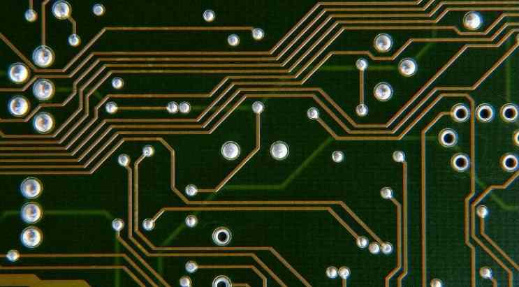
Modern PCBA electronic assembly is a complex process, in the process of production, due to PCB substrate, PCB board processing process factors lead to PCB defects. Next, Xiaobian will introduce some common PCB defects and the causes.
In the process of PCB manufacturing, common PCB defects are: white spots, microcracks, bubbles, delamination, wet weaving, exposed fabric, halo and solder resistance defects.
1. White spots
At the point of glass fiber interleaving on the surface of the plate, the resin is separated from the fiber, and white spots or "cross lines" appear under the surface of the substrate.
Reasons: (1) the plate withstands the impact of inappropriate mechanical external force caused by the separation of local resin and glass fiber into white spots.
(2) The infiltration of fluorine-containing chemicals into the local metal plate erodes the woven points of the glass fiber fabric, forming regular white spots (more serious can be seen as square).
(3) plate by improper thermal stress will also cause white spots, white spots.
2. Micro crack
Microcracks are defined as continuous white spots or "cross marks" occurring within the laminated substrate.
Reason: Mainly affected by mechanical stress, microcracks occur in the laminated substrate.

3. Foaming
Image of local separation caused by local expansion between layers of substrate or between substrate and conductive foil or between substrate and protective coating.
Reasons: (1) surface pollution (oxidation, oil stains, glue stains, other alkaline pollution)
(2) The post-curing time is insufficient, most of the performance is a corner on both sides of the foam off the oil, is found after spraying tin.
(3) The tin is not clean, there is a thin layer of tin on the board, to spray tin, the tin on the board after high temperature melting will put the ink up, forming a bubble.
(4) the water vapor in the hole is not dried on printing ink. After spraying the tin, it will form a ring of bubbles at the edge of the hole where the water is stored
(5) In the PCB board welding process, there is water vapor in the board, in the over-reflow welding is easy to occur bubbles.
4. Layering
Imagination of separation between substrate layers, insulating substrate and any layer within a conductive or multilayer plate.
Cause: (1) The laminating parameters are not set according to the specification requirements
(2) Cleaning is not in place, and there are sundries on the board surface, resulting in stratification after welding.
5. Wet weaving
An unbroken braided fiber completely covered with resin in the substrate, presenting a braided pattern on the surface.
6. Expose fabric
The appearance of braided fibers that have not been fully covered or broken by resin on the surface of the substrate.
7. Halo
Damage or layering on or below the surface of the substrate is usually manifested in a whitened area around the hole or other machining parts.
Reasons: (1) The machine or electric board is not smooth, and there is a gap between the board and the electric board.
(2) the plate is warped and deformed, and there are gaps between the plates
(3) milling cutter wear
(4) The inspector is not clear about the second drill halo standard missed inspection.
8. Welding resistance defects
Solder resistance film is a heat-resistant coating material. Solder resistance defects tend to lead to solder deposition in non-welding areas during PCB welding.
Reason: (1) The spacer or air gap around the pad feature is too large
(2) After welding resistance printing, the drying time and temperature of the plate are not enough, resulting in incomplete welding resistance curing. After high temperature impact in the furnace, the welding resistance layer bubbles.
These PCB defects are important factors affecting the defective rate of electronic products. By understanding these defects and their causes, the process can be improved in the process of electronic assembly and the yield of products can be increased.
PCB process fault analysis: drill bit is easy to break
PCB process fault: the drill is easy to break
Reasons:
(1) Excessive deflection of the main shaft
(2) Improper drilling operations
(3) Improper drill selection
(4) The speed of the bit is insufficient, and the feed rate is too high
(5) The number of stacking layers is too high
(1) The main shaft should be repaired and restored to its original state.
(2)A: Check whether the pressure beriberi pipeline is blocked
B: Adjust the pressure of the pressure foot according to the bit status
C: Check the variation of spindle speed
D: Check the stability of the spindle during drilling operation
(3) Detect the geometry of the bit, wear condition and choose the bit with appropriate length of deschasting slot.
(4) Select the appropriate feed amount to reduce the feed rate.
(5) Reduce to the appropriate number of layers.


Достаточно загрузить файлы Gerber, BOM и проектные документы, и команда KINGFORD предоставит полное предложение в течение 24 часов.