
Контрактное производство электроники под ключ в Китае
Шэньчжэнь, район Баоань, улица Фуюн, улица Фуцяо, район 3, промышленный парк Лонгхуй 6

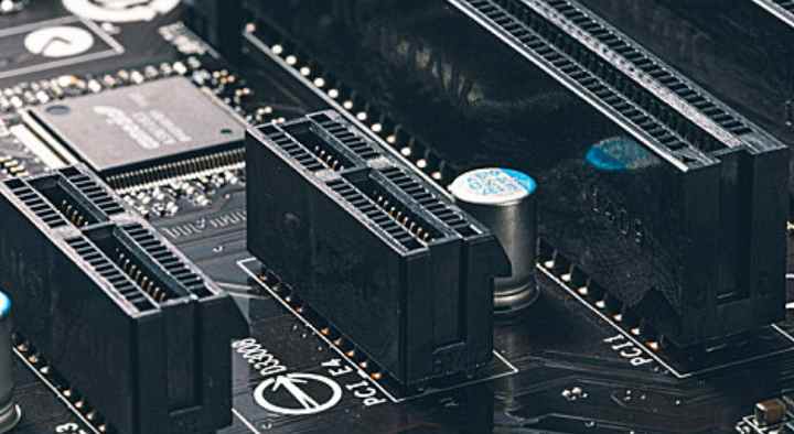
With the evolution of The Times, the progress of science and technology, the requirements of environmental protection, the electronics industry also with the era of the giant wheel initiative or forced forward, the technology of circuit board is not so. Here are several circuit board surface treatment is currently more common process, I can only say that there is no the most perfect surface treatment, so there are so many choices, each of the surface treatment has its own advantages and disadvantages, the next interview list.
Hot air solder is smooth
HASL is the main lead surface treatment process used in the industry. The process is formed by immersing the board in a lead-tin alloy. Excess solder is removed by a "wind knife", which blows hot air over the surface of the board. For PCA, HASL has many advantages: it is the cheapest PCB and the surface layer can be soldered after repeated reflow, cleaning and storage. For ICT, HASL also offers a process for solder auto-covering test pads and through holes. However, HASL surfaces have poor flatness or homogeneity compared to existing alternatives. There are several lead-free HASL replacement processes that are gaining popularity due to the natural substitution nature of HASL. HASL has worked well for many years, but with the requirement for "eco-friendly" green processes, its days are numbered. In addition to the lead-free problem, increasing board complexity and finer spacing have exposed many limitations to the HASL process.

Advantage: Lowest cost PCB surface process, maintains weldability throughout manufacturing process, has no negative impact on ICT.
Disadvantages: Lead-based processes are commonly used, which are now limited and will eventually be eliminated by 2007. For fine pin spacing (< 0.64mm), may cause solder bridging and thickness problems. Surface unevenness can lead to homogeneity problems in the assembly process.
Organic solder protector
Organic solder Protector (OSP) is used to produce a thin, uniform protective layer on the copper surface of the PCB. This coating protects the circuit from oxidation during storage and assembly operations. This process has been around for a long time, but has only recently gained popularity with the search for lead-free technology and fine-spacing solutions.
Osps have better performance than HASL for PCA assembly in terms of coplanar and weldability, but require significant process changes in the type of flux and number of thermal cycles. Careful treatment is required because its acidic properties reduce OSP properties and make copper prone to oxidation. Assemblers prefer to work with metal surfaces that are more flexible and can withstand more thermal cycles.
The use of OSP surface treatment, if the test point is not soldered, will result in contact problems with the pin bed fixture in the ICT. Simply changing to a sharper probe type to pass through the OSP layer will only result in damage and puncturing the PCA test pass hole or test pad. Studies have shown that switching to a higher probe force or changing the probe type has little effect on the yield. Untreated copper has yield strength an order of magnitude higher than with lead welded, and the only result will be damage to the exposed copper test pad. All testability guidelines strongly recommend against direct detection of exposed copper. When using OSPs, you need to define a set of OSP rules for the ICT phase. The most important rule requires that the Stencil be opened at the beginning of the PCB process to allow the solder paste to be added to those test pads and holes that the ICT needs to contact.
Advantages: Comparable to HASL in unit cost, good coplanicity, lead-free process, improved weldability.
Disadvantages: The assembly process requires major changes. If probing raw copper surfaces is detrimental to the ICT, over-pointed ICT probes may damage the PCB, requiring manual preventive treatment, limiting ICT testing and reducing repeatability of testing.
No plating nickel gold immersion
Nickel plating free gold immersion (ENIG) is a coating that has been used successfully on many circuit boards and has a flat surface and excellent weldability despite its high unit cost. The main disadvantage is that the non-plated nickel layer is very fragile and has been found to crack under mechanical pressure. This is known in the industry as a "black block" or "mud crack", and has led to some bad press from ENIG.
Advantages: Good weldability, flat surface, long storage life, can withstand many reflow welding.
Cons: High cost (about five times as much as HASL), "black block" issues, manufacturing processes that use cyanide and other harmful chemicals.
Silver immersion
Silver immersion is a new addition to PCB surface treatment. It is mainly used in Asia and is gaining popularity in North America and Europe.
During welding, the silver layer melts into the solder spot, leaving a tin/lead/silver alloy on top of the copper layer that provides a very reliable solder spot for the BGA package. Its contrasting color makes it easy to inspect, and it is a natural alternative to HASL in welding treatments.
Silver immersion is a promising surface processing technology, but as with all new surface technologies, end users are very conservative about it. Many manufacturers refer to this process as an "under investigation" process, but it is likely to be the best choice for lead-free surfaces.
Pros: Good weldability, flat surface, natural alternative to HASL immersion.
Cons: The conservative attitude of end users means there is a lack of relevant information in the industry.
This is a relatively new surface treatment process that has many similar properties to the silver immersion process. However, there are significant health and safety concerns to be taken into account as thiourea, a possible carcinogen, is used in the tin immersion process of PCB manufacturing. In addition, tin migration (the "tin burr" effect) is of concern, although anti-migration chemicals have had some success in controlling this problem.
Advantages: Good weldability, flat surface, relatively low cost.
Cons: Health and safety issues, limited number of thermal cycles.


Достаточно загрузить файлы Gerber, BOM и проектные документы, и команда KINGFORD предоставит полное предложение в течение 24 часов.