
Контрактное производство электроники под ключ в Китае
Шэньчжэнь, район Баоань, улица Фуюн, улица Фуцяо, район 3, промышленный парк Лонгхуй 6

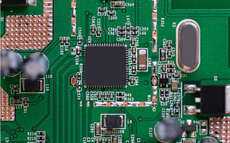
The PCB processing process from the inner line pattern transfer of PCB substrate to the outer line pattern transfer by pressing several times will cause different growth and contraction of the warp and weft of the board. From the FLOW-CHART of the entire PCB production, we can find out the reasons and processes that may cause abnormal expansion and shrinkage of board parts and poor size consistency:
1. PCB substrate incoming dimensional stability factors PCB substrate incoming dimensional stability, especially the dimensional consistency between each laminating CYCLE of the supplier. Even though the dimensional stability of PCB substrate in different cycles of the same specification is all within the specification requirements, the poor consistency between them may cause the out-of-tolerance of the graphic size of the subsequent batch production of PCB substrates due to the difference between different batches of board materials after the first plate trial production has determined a reasonable inner layer compensation. At the same time, there is a material anomaly in the transfer of the outer pattern to the shape of the process found in the board shrinkage. During the production process, it was found that the width of the slab and the length of the shipping unit had a serious shrinkage in relation to the outer pattern transfer ratio of 3.6mil/10inch during the pre-shape processing data measurement for some batches of the sheet. After tracing, the X-RAY measurement and outer pattern transfer ratio of this abnormal batch of plates after outer layer compaction are both within the control range. At present, no good method has been found for monitoring the process monitoring.
2. Factors of split-board design mode The conventional split-board design is symmetrical, and has no obvious influence on the graphic size of finished PCB board under the condition of normal graphic transfer ratio. However, in order to improve the utilization rate of board materials and reduce the cost, a part of the board uses the design of asymmetric structure, which will bring a very obvious impact on the consistency of the graphic size of finished PCB in different distribution areas. Even in the process of PCB processing, we can find that the alignment of the plate with this kind of asymmetric design is more difficult to control and improve than the conventional plate in the process of laser blind hole drilling and outer pattern transfer exposure/flux resistance exposure/character printing.
3, the first inner graphics transfer process factors the first inner graphics transfer process plays a very key role in whether the finished PCB board size meets customer requirements. For example, if there is a large deviation in the film ratio compensation provided by a transfer of inner LAYER graphics, it will not only directly lead TO the failure of the finished PCB graphic size to meet customer requirements, but also cause the subsequent abnormal alignment between the laser blind hole and the bottom connecting disk, resulting in decreased insulation performance between LAYER TO LAYER and even short circuit. And the pass/blind hole alignment problem in the process of outer pattern transfer.
Based on the above analysis, we can take appropriate measures to monitor and improve anomalies.
1. Monitoring the dimensional stability of PCB substrate incoming materials and the consistency of size between batches The dimensional stability of PCB substrate supplied by different suppliers is tested regularly to track the difference of longitude and latitude data between different batches of board material of the same specification, and the PCB substrate test data can be analyzed by appropriate statistical techniques. In this way, suppliers with relatively stable quality can be identified, and more detailed supplier selection data can be provided for SQE and purchasing department. The severe shrinkage of PCB parts after the transfer of the outer pattern caused by the poor dimensional stability of PCB substrates in individual batches can only be detected by the measurement of the outer pattern production first plate or during the shipment review. However, the latter has higher requirements for batch management, and it is easy to appear mixed plate in mass production of a certain number.
2, the design of the symmetrical structure of the jointed board design should be as far as possible to use the design of the symmetrical structure, so that the growth and contraction of each shipping unit in the board remain relatively consistent. If possible, communicate with the customer to advise them to allow specific identification of the location of each shipping unit within the assembly board by means of etch/character identification on the process edge of the board. The effect of this method will be more obvious in the plate with asymmetric design. Even if the size of each unit in each plate is out of tolerance due to the graphic asymmetry, or even the partial blind hole bottom connection anomaly caused by it, it can be very convenient to determine the abnormal unit and pick it out before shipment, so as not to flow out and cause the customer to complain about the abnormal packaging.
3. Make the ratio of the first inner graph transfer ratio and scientifically determine the ratio of the first inner graph transfer ratio. Make the ratio of the first inner graph transfer ratio and scientifically determine the ratio of the first inner graph transfer ratio of the production plate. This is particularly important when changing PCB substrates or P-chips from other suppliers to reduce production costs. When the plate is found out of the control range, it should be processed according to whether the unit pipe position hole is secondary drilling. If the plate is a conventional processing process, it can be released to the outer graphic transfer according to the actual situation through appropriate adjustment of film multiplier; In the case of secondary drilling plates, special care should be taken to handle abnormal plates to ensure that the graphic size of finished plates is the distance between the target and the pipe hole (secondary drilling); Attached is a list of first plate multipliers of secondary laminates.
4. PCB manufacturing process monitoring uses the inner layer target data of the outer layer or the sub-outer layer of the plate measured in the X-RAY production of drilling pipe position holes after its lamination, analyzes whether it is within the control range and compares it with the corresponding data collected from the qualified first plate to judge whether the size of the plate is abnormal. According to theoretical calculation, the ratio should be controlled within +/-0.025% in order to meet the size requirements of conventional plate parts.


Достаточно загрузить файлы Gerber, BOM и проектные документы, и команда KINGFORD предоставит полное предложение в течение 24 часов.