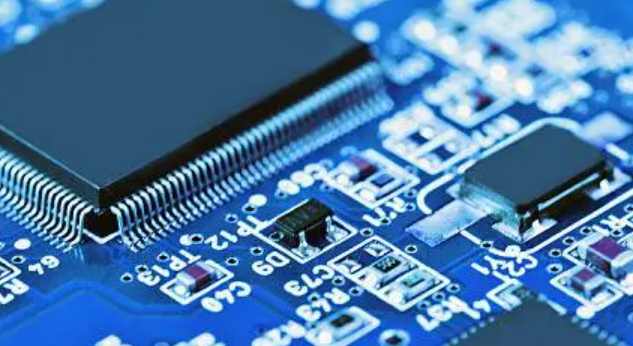
PCB board is the PCB according to a certain arrangement of several pieces of splicing together, convenient SMT, improve welding efficiency.
1 Why do we need to assemble the board
1. To meet the demand of production. Some PCB boards are too small to meet the requirements of fixture making, so they need to be pieced together for production.
2. Improve the welding efficiency of SMT patches. Only one SMT is required to complete the welding of multiple PCB.
3. Improve cost utilization. Some PCB board is shaped, the board can be more efficient use of PCB board area, reduce waste, improve the utilization rate of cost.
2. What are the ways of panel design?
1.V-CUT
V-CUT is to draw a slot at the joint of two boards, as long as the two boards are put together, leaving some space between them (generally 0.4mm), but the connection of the board in this place is relatively thin, easy to break, the edges of the two boards need to be merged together.
V-CUT is generally a straight line, without complex routing such as curved arc. Try to assemble the board in a straight line.
2. Stamp holes
For irregular PCB board, such as circular, V-CUT is not possible, at this time, stamp holes need to be used to connect the plate, so stamp holes are generally used in the special-shaped board.
The edges of the two boards are connected by a small piece of board, and the small piece of board has many holes where the two boards join, which is easy to break. When broken off, the edges of the board look like the edges of a stamp, so this arrangement is called a stamp hole.
3. Hollow connection bar
The hollow connection bar is used more in the board with a half hole process. It is the use of a very narrow plate to connect, which is similar to the stamp hole. The difference is that the connection part of the connection bar is a little narrower, and there is no hole on both sides.
There is one disadvantage of the splicing method of the hollow joint: the splicing will have a very obvious convex point. Stamp holes also have raised spots, which are less noticeable because they are separated by the holes.
One might think that why use a hollow connection bar instead of a stamp hole? This is because when the module is made with half holes all around, neither the stamp hole nor the V-CUT can be used, and only hollow connecting strips can be connected at the four corners of the module.
3. What are the principles of the board?
In order to facilitate production, as far as possible to keep the board behind the assembly square shape. In short, don't let the ratio gap too big.
4 Spacing requirements
1. For PCB whose outermost part is less than 3mm from the edge of the board, a process edge must be added, usually the longer edge is used as the process edge;
2. Leave a space of more than 0.5mm between the components and the V-cut to ensure the normal operation of the tool.
There are many design and manufacturing factors to consider when determining PCB board thickness, such as:

Copper thickness
plate
The number of PCB layers
Signal type
Type of through-hole
Operating environment
Manufacturing factors that affect PCB thickness include:
Technological capability of drilling equipment
Copper thickness
Number of layers
Split-board method
Factors to consider when designing PCB with non-standard thickness:
1. Process capacity of plate factory
The first thing to consider is whether your board factory has the equipment to make the boards the thickness you need. This decision should be made early in the design process, taking into account other relevant DFM design requirements. Otherwise, you may be forced to make modifications and redesign your PCB stack structure.
2. Extend delivery time
If you choose materials that are not available at the board factory, the PCB production cycle will often be prolonged. Therefore, delivery time should be taken into account for non-standard plate thickness.
3. Additional costs
This is probably the most important point, you need to assess the cost of the special sheet, the additional manufacturing cost, and the cost of extended delivery time to determine whether the additional cost is acceptable.
Giving preference to standard PCB thicknesses will make your boards faster and cheaper to manufacture. However, if you decide to choose non-standard thickness, you should first communicate with the board manufacturer before starting the PCB design to ensure that the process can be manufactured, and to communicate delivery times and additional manufacturing costs.


