
Контрактное производство электроники под ключ в Китае
Шэньчжэнь, район Баоань, улица Фуюн, улица Фуцяо, район 3, промышленный парк Лонгхуй 6


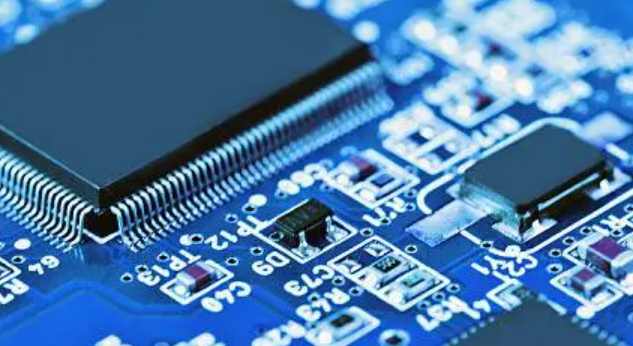
In the circuit boardsurface treatment has a very common use of the process, called gold. The purpose of gold sinking process is to deposit stable color, good brightness, smooth coating and good weldability nickel gold coating on the surface of PCB printed circuit.
Simply put, gold deposition is the use of chemical deposition method, through chemical REDOX reaction on the circuit board surface to produce a layer of metal coating.
First, the role of gold sinking process
The copper on the circuit board is mainly copper, copper solder joints in the air is easy to be oxidized, which will cause electrical conductivity is to eat tin poor or poor contact, reduce the performance of the circuit board, then you need to surface treatment of copper solder joints, gold is gilded above, gold can effectively block copper metal and air to prevent oxidation, So sinking gold is a kind of surface oxidation prevention treatment, is covered with a layer of gold on the surface of copper by chemical reaction, also known as gold.
Two, sinking gold can improve the surface treatment of PCB board
The advantage of the gold plating process is that the deposition color on the surface of the printed line is very stable, the brightness is very good, the coating is very smooth, and the weldability is very good. The thickness of sunk gold is generally 1-3 Uinch, so the surface treatment of sunk gold is generally thicker, so the surface treatment of sunk gold is widely used in key board, gold finger board and other circuit boards, because gold has strong conductivity, good oxidation resistance and long service life.

Three, the advantages of the use of gold-plated circuit boards
1, the gold plate bright color, good color, good-looking, enhance the attraction to customers.
2. The crystal structure formed by sinking gold is easier to weld than other surface treatments, which can have better performance and ensure quality.
3. Because the gold plating only has nickel gold on the pad, it will not affect the signal, because the signal transmission in the skin effect is in the copper layer.
4, the metal properties of gold are relatively stable, the crystal structure is more dense, not easy to occur oxidation reaction.
5, because the gold plate only has nickel gold on the welding plate, so the welding resistance on the line and the combination of copper layer is more firm, it is not easy to cause micro short circuit.
6, the project will not affect the distance when making compensation, facilitate the work.
7, the stress of the gold plate is easier to control, and the experience is better in use.
Four, the difference between gold and gold fingers
Goldfinger, let's put it bluntly, is a brass contact, or a conductor. Specifically, because of the strong oxidation resistance of gold, and also very strong conductivity, so on the memory bar and memory slot connected to the parts plated gold, then all signals are transmitted through the gold finger. Goldfingers get their name because they are made up of numerous yellow conductive contacts that are plated and arranged like fingers. Colloquially speaking, the gold finger is the connection between the memory bar and the memory slot, and all the signals are transmitted through the gold finger. A goldfinger is made up of a series of electrically conductive contact plates of gold, which are actually coated with gold by a special process.
Therefore, the simple distinction is that the gold is a surface treatment process of the circuit board, and the gold finger is the circuit board with signal connection and conduction components. In the reality of the market, the goldfinger does not really appear to be gold. Because of the high price of gold, at present more memory are replaced by tin plating, since the 1990s began to popularize tin material, the current motherboard, memory and graphics card and other equipment "gold finger" is almost all made of tin material, only part of the high performance server/workstation accessories contact point will continue to use gold plating, the price is naturally expensive.
Test method
Needle bed method
This method consists of a probe with a spring attached to each detection point on the circuit board. The spring gives each probe 100-200g of pressure to ensure good contact at each detection point. Such probes are arranged together in a "needle bed". Under the control of the detection software, the detection points and signals can be programmed. Figure 14-3 is a typical structure of a needle bed tester, and the tester can know the information of all the test points. The probes are actually installed only for the test points that need to be tested. Although it is possible to inspect both sides of the board at the same time using the needle bed test method, it is advisable to design the board so that all inspection points are on the welded side of the board. Needle bed tester equipment is expensive and difficult to maintain. Different arrangements of needles are selected according to their specific application.
A basic general-purpose grid processor consists of a drilled board with pins with center spacing of 100, 75, or 50mil. The pins act as probes and make direct mechanical connections using electrical connectors or nodes on the circuit board. If the pad on the circuit board matches the test grid, the polyvinegar film, perforated to specification, is placed between the grid and the circuit board to facilitate the design of a specific probe. Continuity detection is achieved by accessing the end point of the grid, which has been defined as the x-y coordinates of the pad. Since every network on the circuit board is checked for continuity. Thus, an independent test is completed. However, the proximity of the probes limits the effectiveness of the needle-bed method.
SMT patch processing basic introduction
2023-03-30


Достаточно загрузить файлы Gerber, BOM и проектные документы, и команда KINGFORD предоставит полное предложение в течение 24 часов.