
Контрактное производство электроники под ключ в Китае
Шэньчжэнь, район Баоань, улица Фуюн, улица Фуцяо, район 3, промышленный парк Лонгхуй 6

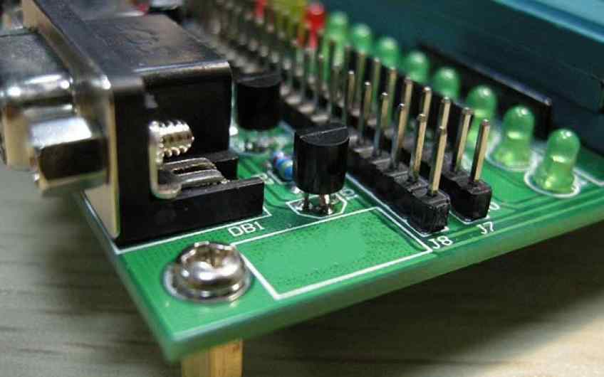
kingford is a professional PCB design company engaged in electronic products layout layout design, mainly undertake multi-layer, high density PCB design and circuit board design proofing business. Next, we introduce the common problems in PCB design.
First, pad overlap
1. The overlap of pads means the overlap of holes, which is caused by drill bit damage and hole damage caused by drilling multiple holes in one position during the drilling process.
2. The two holes on the multilayer plate overlap.
Two, graphic layer abuse
1. Some useless connections are made on some graphics layer.
2. PCB design requires fewer lines.
3. It violates the traditional design, such as the surface design of the parts at the bottom and the welding surface design at the top, which causes inconvenience.
3. Random placement of characters
1. The patch welding pad of character cover brings inconvenience to the on-off test of circuit board and the welding of components.
2. The character design is too small, making screen printing difficult. Too large will overlap the characters and make them difficult to distinguish.
4, single pad aperture setting
1. Single side pad is usually not drilled. If drilling holes need to be marked, the hole diameter should be designed to be zero.
2. Single pad should be specially marked for drilling.
5. Drawing board with filling block
When flux resistance is applied, the filler block area will be covered with flux resistance, resulting in difficulty in welding the device.
6, the formation of electricity is the flower pad and connection
Because the power supply is designed in a flower-pad pattern, the ground layer is relative to the image on the actual printed plate, and all connection lines are isolation lines. When drawing isolation lines for groups of power supplies or types of ground, no gaps should be left to short circuit or block the connection area between groups of power supplies.
7, processing grade definition is not clear
1. Board design is on the top layer. If the front and back are not stated, the manufactured panel may be fitted with devices rather than welded.
2. For example, when designing a four-layer board, the top layer, the middle layer, the middle layer and the bottom layer are used, but they are not arranged in this order in the processing.
8, PCB design in the filling block is too much or the filling block is filled with very fine lines
1. There is data loss and incomplete data in the lighting drawing.
2. In the process of optical rendering data processing, the filling blocks are drawn line by line, so the amount of data generated is quite large, which increases the difficulty of data processing.

Nine, surface mount device welding pad is too short
For too dense surface mount devices, an up - down (left - right) staggered position must be used in order to mount the test pins.
Ten, large area grid spacing is too small
The edges between the same lines that make up the large area of grid lines are too small (less than 0.3 mm) and many of the broken films are easily attached to the circuit board after the image is displayed, resulting in broken lines.
11. Large area of copper foil is too close to the outer frame
The distance between the large area of copper foil and the outer frame should be at least 0.2 mm.
Twelve, outline frame design is not clear
Some customers design contours in the retention layer, board layer, top layer, etc., which makes it difficult for board manufacturers to determine which contour line should prevail.
Thirteen, the graphic design is not unified
The uneven coating will affect the quality of graphic electroplating.
14. Abnormal hole is too short
The length/width of the special-shaped hole should be ≥ 2:1, and the width should be greater than 1.0mm, otherwise the drilling machine is easy to break during processing, and the processing is difficult and the cost will be increased.
2. What is the cause of PCB board breakage?
If you want to make a complete PCB board, you need to go through multiple complicated processes. If there are some operational mistakes in the production process of PCB board, it will lead to quality problems in the final production of the finished board, which does not meet the requirements of the product. The common PCB board breaking problem will affect the realization of the circuit board function.
Then, what is the cause of PCB board break?
1, the film processing: the film is not firm, there are bubbles, if the wet film will be garbage pollution.
2. Exposure process: problems caused by scratches or garbage on the negatives, including problems with the exposure machine and insufficient local exposure.
3. Developing process: the development is fuzzy and unclear.
4, etching process: nozzle pressure is too large, etching time is too long.
5, electroplating problems: when electroplating uneven plating or surface adsorption force.
6. Improper operation: During the production of the circuit board, the circuit board is scratched and broken due to improper operation.
What is the cause of PCB board wire breakage? Firstly, take a look at the form of wire breakage, and find out which process caused the PCB board wire breakage problem by analyzing the form of wire breakage, and then gradually investigate the possible causes in the production process.
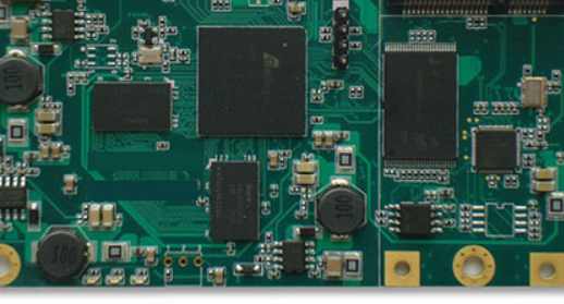
PCB board advantage
Energy production from 2 layers to 14 layers, 14-22 layers can be proofing production.
Minimum line width/spacing: 3mil/3milBGA Spacing :0.20MM
Minimum aperture: 0.1mm Size :610mmX1200mm
Ink: Tamura, Taiyo, Fudoken;
FR4: Shengyi, Kingboard, Harbour, Hongren, Guoji, Hezheng, Nanya,
(Shengyi S1130/S1141/S1170),Tg130℃/ Tg170℃ T g180℃ and other high TG plates)
High frequency plate: Rogers, Taconic, ARLLON;
Surface process: tin spray, lead-free tin spray, gold plating, full plate gold plating, plug gold plating, full plate thick gold, chemical tin (silver), anti-oxidation (OSP) blue glue, carbon oil
Why choose Shenzhen kingford?
1. Strength guarantee
▪SMT workshop: We have imported SMT machines and several sets of optical inspection equipment, with a daily output of 4 million. Each process is equipped with QC personnel, who can keep an eye on product quality.
▪DIP production line: We have two wave-soldering machines, among which there are more than 10 old employees who have worked for more than three years. The skilled workers can weld all kinds of plug-in materials.
2. Quality assurance, cost-effective
▪ High-end equipment can stick precision shaped parts, BGA, QFN, 0201 materials. Can also template patch, loose material hand.
▪ Sample and size batch can be produced, proofing from 800 yuan, batch 0.008 yuan/point, no start-up fee.
3. Rich experience in SMT and welding of electronic products, stable delivery
▪ Accumulated SMT SMT processing services for thousands of electronic enterprises, involving many kinds of automotive equipment and industrial control motherboard. The products are often exported to Europe and the United States, and the quality can be affirmed by new and old customers.
▪ On time delivery, normal 3-5 days after complete materials, small batch can also be expedited on the same day shipment.
4. Strong maintenance ability and perfect after-sales service
▪ Experienced maintenance engineers can repair all kinds of patch welding caused by bad products, to ensure the connection rate of each piece of circuit board.
▪ 24-hour customer service staff at any time response, the fastest speed to solve your order problems.


Достаточно загрузить файлы Gerber, BOM и проектные документы, и команда KINGFORD предоставит полное предложение в течение 24 часов.