
Контрактное производство электроники под ключ в Китае
Шэньчжэнь, район Баоань, улица Фуюн, улица Фуцяо, район 3, промышленный парк Лонгхуй 6

After passing through the automatic tin furnace, the insulation green paint of PCB under the plate line will peel off. I don't know why?
After passing through the automatic tin furnace, the insulation green paint of PCB under the plate line will peel off. I don't know why? What are the reasons for S/M Peeling after gold?
There are three big possibilities for green paint to fall off. The first is that the nature of green paint itself is not enough to withstand the test of tin furnace, which may be caused by the expiration of green paint or poor operation. Almost all green paints used by the industry are tested for heat resistance, reliability, etc., so there should not be a problem regularly. In this regard, review whether the material itself has changed or whether the process has changed.
The second may be the influence of external force, including flux supply and mechanical collision, especially in the high temperature condition green paint characteristics are no longer like the normal temperature environment with high hardness, at this time the board of green paint by any external impact is easy to produce scratches and flaking.
The third big possibility is that the circuit board in the green paint coating or storage caused by moisture absorption burst, water gas in the heat gasification volume expanded nearly three hundred times, instant temperature rise and green paint softening, it is very easy to make the green paint peel. This kind of problem will appear in the process of the board production of tin spray, may also occur in the wave welding, back welding and other assembly process.
There are several possibilities for SMPEELING after gold, the first is that copper is not ideal before processing, the second is that drying is not enough before S/M coating, the third is that the stagnation time is too long to produce oxide layer, the fourth is that the green paint itself is not good material suitable for gold processing, the fifth is that the green paint is not polymerization enough. Sixth, it may also occur if you do more than one high temperature process, such as gold leaching and gold plating together or twice. You have to do a detailed analysis to clarify item by item because there are many possibilities, but in general usage is quite important for the S/M category.

Some special green paint, the reaction to UV light is slow, need oxygen and relatively high exposure energy to achieve high degree of polymerization. If the exposure degree of polymerization is insufficient, the subsequent baking will not be able to fully achieve the due strength of polymerization. If this kind of material is used, the operator should be clearly informed of the correct handling method, otherwise the problem will continue. The above is for your reference.
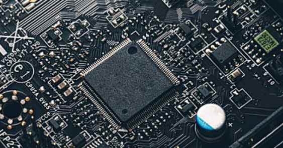
Understand the meaning and design principles of PCB multilayer board
PCB's are single - sided, double - sided and multilayer. For simple electrical appliances such as radios, use single - sided PCB's. However, with the progress of The Times, both function and volume, electronic products need to be updated. For multifunctional, small size electronic products, single and double sided PCB can not fully meet the requirements, but must use multi-layer PCB.
Multilayer PCB has many advantages, such as: high assembly density, small size; The wiring between electronic components is shortened, the signal transmission speed is fast, and the wiring is convenient; Good shielding, etc. There is no limit to the number of layers of multilayer boards. At present, there are more than 100 layers of PCB, and the common ones are four and six layers of boards.
Multilayer board in the design, each layer should maintain symmetry, and it is best to even copper layer, if not symmetrical, easy to cause distortion. The wiring of multilayer board is carried out according to the function of the circuit. When wiring the outer layer, more wiring is required on the welding surface and less wiring on the component surface, which is conducive to the maintenance and troubleshooting of printed board. In routing, the power layer, ground layer and signal layer should be separated to reduce the interference between the power, ground and signal. The lines of the adjacent two layers of printed boards should be perpendicular to each other as far as possible or diagonal lines, curves, not parallel lines, in order to reduce the interlayer coupling and interference of the substrate.
Compared with single-sided and double-sided PCB, which layers are composed of? What does each layer represent and what is its use? Multilayer PCB is mainly composed of the following Layers: Signal Layers (signal layer), InternalPlanes (internal power supply), Mechanical Layers (mechanical layer), Masks (welding resistance layer), Silkscreen (Silkscreen), and System (system working layer).
The signal layer is divided into top layer, middle layer and bottom layer, which is mainly used to place various components, or for wiring and welding. The internal power layer, also known as the internal power layer, is dedicated to arranging power cables and ground cables. The mechanical layer is generally used to place the indicative information about board making and assembly methods, such as the physical size line of the circuit board, data data, hole information, etc. The solder stop layer also has a top layer and a bottom layer on which the pad or other object placed is a copper-free area. The screen printing layer is mainly used to draw the outline of the component, the number of the placed component or other text information, while the system working layer is used to display the information that violates the design rule check.


Достаточно загрузить файлы Gerber, BOM и проектные документы, и команда KINGFORD предоставит полное предложение в течение 24 часов.