
Контрактное производство электроники под ключ в Китае
Шэньчжэнь, район Баоань, улица Фуюн, улица Фуцяо, район 3, промышленный парк Лонгхуй 6


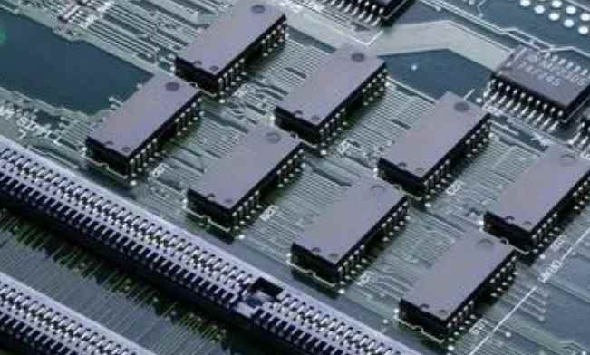
one Basic knowledge of PCB holes
Through hole (via) is one of the important components of multilayer PCB, the cost of drilling usually accounts for 30% to 40% of the PCB board. Through the hole action can be divided into the electrical connection between each layer and used as a device fixing or positioning two categories. through holes in the process are generally divided into three categories, namely blind via, buried via and through via. Blind holes are located on the top and bottom surfaces of the PCB and are of a certain depth. They are used to connect the surface circuit to the inner circuit below. The depth of the holes usually does not exceed a certain ratio (aperture).
Buried holes are connection holes located in the inner layer of the printed circuit board that do not extend to the surface of the board. Both types of holes are located in the inner layer of the circuit board, which is completed by a through-hole molding process prior to lamination. Several inner layers may be overlapped during the through-hole formation process. The third type, called through-holes, runs through the entire circuit board and can be used for internal interconnection or as installation positioning holes for components. Because the through hole in the process is easier to achieve, the cost is lower, so most of the printed circuit board are using it, rather than the other two through holes. From a design point of view, a through hole is mainly composed of the drill hole in the middle and the pad area around the drill hole. The size of these two parts determines the size of the through hole. The smaller the hole, the smaller its own parasitic capacitance, suitable for high-speed circuits. But as the holes get smaller, they cost more and are limited by technology such as drilling and plating on their plating.

Two. About the parasitic capacitance through the hole
The parasitic capacitance through the hole itself has stray capacitance to the parasitic ground. The main effect of the parasitic capacitance through the hole on the circuit is to prolong the rise time of the signal and reduce the speed of the circuit. Although the effect of the parasitic capacitance of a single through-hole is not obvious, the designer should be careful if multiple through-holes are used to switch between layers.
Three. On the parasitic inductance through the hole
In the design of high-speed digital circuit, the harm caused by the parasitic inductance is often greater than the influence of the parasitic capacitance. Its parasitic series induction will weaken the contribution of the bypass capacitor and reduce the filtering effectiveness of the whole power system. The diameter of the hole has little effect on the inductance, while the length of the hole has the biggest effect on the inductance. The impedance generated by the hole can no longer be ignored in the presence of high frequency current. In particular, it should be noted that the bypass capacitor needs to pass through two holes when connecting the power layer to the formation, so that the parasitic inductance of the hole will be multiplied.
Four, about the use of holes
1. Considering the cost and signal quality, a reasonable hole size is selected. If necessary, consider using different sizes of holes. For example, for power supply or ground wire, consider using larger sizes to reduce impedance, and for signal wiring, use smaller holes. Of course, as the hole size decreases, the corresponding cost will increase.
2. From the two formulas discussed above, it can be concluded that the use of thinner PCB board is beneficial to reduce the two parasitic parameters through the hole.
3. Try not to change the layer of signal wiring on PCB board, that is to say, try not to use unnecessary holes.
4. The pins of the power supply and the ground should be drilled into the nearest hole. The shorter the lead between the pins and the hole, the better. Multiple holes may be drilled in parallel to reduce equivalent inductance.
5. A number of grounded through-holes are placed near the through-holes of the signal layering to provide the nearest loop for the signal. You can even put some extra ground holes in the PCB board.
6. For high speed PCB boards with high density, you can consider using micro holes.


Достаточно загрузить файлы Gerber, BOM и проектные документы, и команда KINGFORD предоставит полное предложение в течение 24 часов.